
Organic device and method for manufacturing organic device

a technology of organic devices and organic materials, which is applied in the field of organic devices and a method of manufacturing organic devices, can solve the problems of degradation of the s/n ratio, deformation of the optical characteristics of the light guide, and insufficient adhesion between the substrate and the light guide, so as to achieve enhanced adhesion between the substrate and the polymer layer

Inactive Publication Date: 2011-03-03
ORMON CORP
View PDF6 Cites 1 Cited by
  • Summary
  • Abstract
  • Description
  • Claims
  • Application Information

AI Technical Summary

Benefits of technology

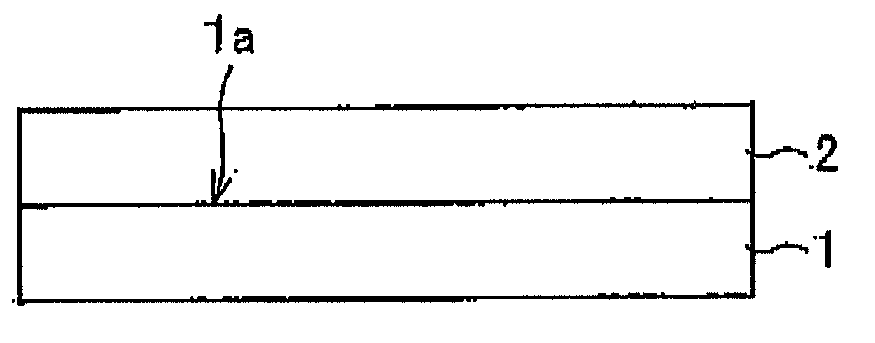
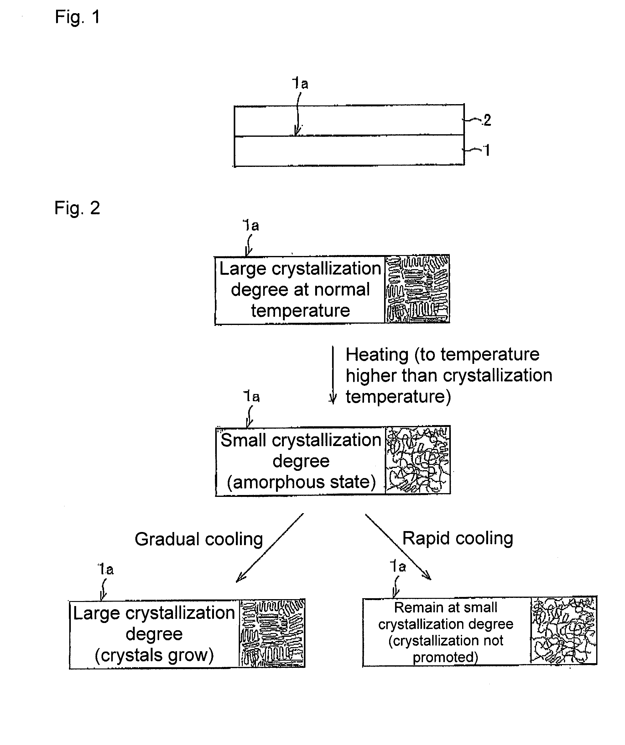
The present invention provides an organic device with a polymer layer on a substrate made of polymer, where the adhesiveness between the substrate and the polymer layer can be enhanced. This is achieved by reducing the crystallization degree of the adhesive surface with the polymer layer in the substrate. The reduced crystallization degree ensures good adhesiveness even under adverse conditions of ultra-bent state or ultra-twisted state. Additionally, the crystallization degree of the interior of the substrate is maintained large, which enhances the pulling resistance property of the structure.

Problems solved by technology

However, the adhesiveness between the substrate and the light guide may not be sufficiently ensured in the light guide placed under adverse conditions such as ultra-bent state or ultra-twisted state.
Thus, if the light guide serving as the organic device is manufactured using the technique described in patent document 1, the optical characteristics of the light guide may degrade as the light guide strips from the substrate.
The variation in the coupling loss leads to degradation of the S / N ratio.
Thus, the loss by the local bending increases, the coupling loss varies, and the S / N ratio degrades.

Method used


Image

  • Organic device and method for manufacturing organic device
  • Organic device and method for manufacturing organic device
  • Organic device and method for manufacturing organic device

Examples


application example

[0117]The optical module 100 of the present embodiment can be applied to the following application examples.

[0118]First, as a first application example, use can be made at a hinge portion in a foldable electronic device such as a foldable portable telephone, a foldable PHS (Personal Handyphone System), a foldable PDA (Personal Digital Assistant), and a foldable notebook computer.

[0119]FIGS. 15(a) to (c) show an example in which the light guide 20 is applied to a foldable portable telephone 40. In other words, FIG. 15(a) is a perspective view showing an outer appearance of the foldable portable telephone 40 incorporating the light guide 20.

[0120]FIG. 15(b) is a block diagram of a portion where the light guide 20 is applied in the foldable portable telephone 40 shown in FIG. 15(a). As shown in the figure, a control unit 41 arranged on a body 40a side in the foldable portable telephone 40, an external memory 42, a camera (digital camera) 43, and a display unit (liquid crystal display) ...


PUM

PropertyMeasurementUnit
inclined angleaaaaaaaaaa
optical functionaaaaaaaaaa
crystallization temperatureaaaaaaaaaa

Abstract

An organic device has a substrate made of polymer, and a polymer layer adhered on the substrate. A crystallization degree of an adhesive surface with the polymer layer in the substrate is smaller than a crystallization degree of an interior of the substrate. In a manufacturing method for manufacturing an organic device including a substrate made of polymer; and having a polymer layer adhered on the substrate, the manufacturing method includes performing a low crystallization process on an adhesive surface with the polymer layer in the substrate to have a crystallization degree lower than a crystallization degree of an interior of the substrate.

Description

TECHNICAL FIELD[0001]The present invention relates to an organic device and a method of manufacturing the organic device.BACKGROUND ART[0002]In recent years, optical communication network enabling large capacity data communication at high speed is expanding. The optical communication network is assumed to be mounted on a consumer device in the future. An electrical input / output optical data transmission cable (optical cable) capable of being used no different from the present electrical cable is desired for the application of large capacity data transfer at higher speed, noise countermeasures, and data transmission between substrates in the device. In view of flexibility, a light guide is desirably used for the optical cable.[0003]The light guide is formed by a core having a large index of refraction and a clad having a small index of refraction arranged in contact with the periphery of the core, and propagates the light signal entered to the core while repeating total-reflection at...

Claims


Application Information

Patent Timeline
Patent Type & Authority Applications(United States)
IPC IPC(8): G02B6/10B32B27/08B32B7/12
CPCB29B13/023B29C66/91921B29C66/024B29C66/0242B29C66/0244B29C66/0342B29C66/737B29K2023/12B29K2067/00B29K2075/00B29K2079/08B29K2995/0018B29K2995/004B29K2995/0041B29L2011/0066B29L2031/3431B29L2031/767G02B6/1221G02B6/138G02B6/3604G02B6/43H04M1/0214H04M1/026H04M1/22B29C65/8207B29C66/91645B29C66/91411B29C65/00B29C66/91943B29C66/73921B29C66/73774B29C66/45B29C65/1406B29C65/02B29C66/71B29C66/1122Y10T428/31797Y10T428/31511Y10T428/31565Y10T428/31663B29K2067/003B29K2033/08B29K2023/18B29K2023/06
Inventor YOSHITAKE, NAOKITATARA, YOSHITAKAYASUDA, NARUHOSOKAWA, HAYAMI
Owner ORMON CORP
Learn More