
Copper foil provided with dielectric layer for forming capacitor layer, copper clad laminate for formation of capacitor layer using such such copper foil with dielectric layer, and method for producing such copper foil with dielectric layer for formation of capacitor layer

a technology of dielectric layer and copper foil, which is applied in the field of copper foil, can solve the problems of deteriorating product yield, affecting the quality of formed film, and affecting the product yield, so as to achieve uniform thickness, prevent short circuit effectively, and high dielectric constant

Inactive Publication Date: 2006-03-16
MITSUI MINING & SMELTING CO LTD
View PDF2 Cites 14 Cited by
  • Summary
  • Abstract
  • Description
  • Claims
  • Application Information

AI Technical Summary

Benefits of technology

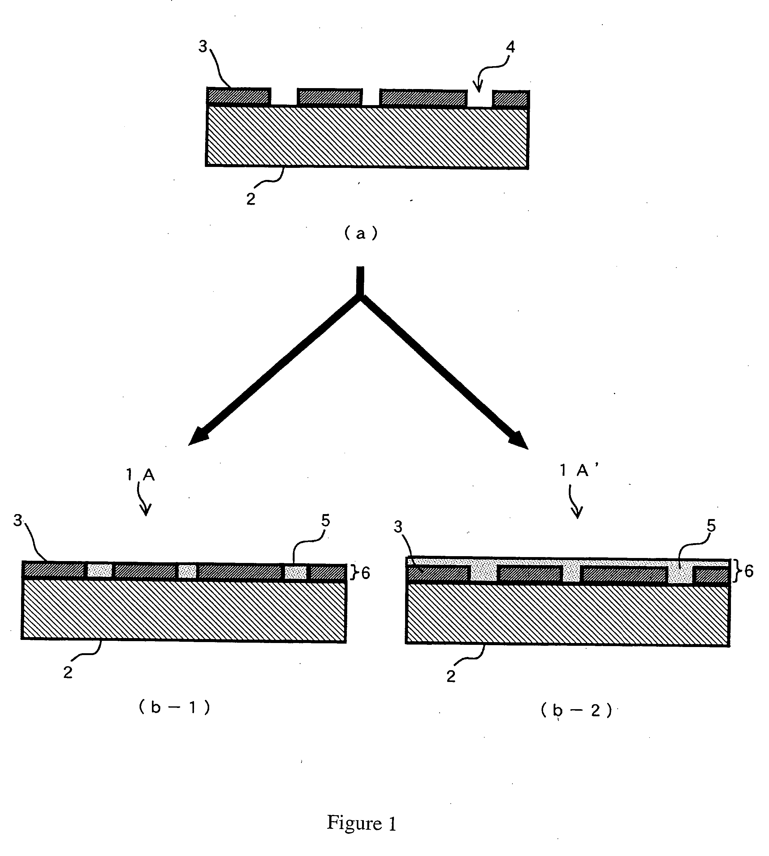
[0079] A dielectric-layer-provided copper foil of the present invention can completely prevent a short circuit between an upper electrode and a lower electrode of a capacitor circuit obtained by using the dielectric-layer-provided copper foil because the copper foil is embedded by a pit-like defective-portion polyimide resin produced on a metal-oxide sputter film having a high dielectric constant even if using the sputter film for the configuration of a dielectric layer. Moreover, when a polyimide resin film covers a metal-oxide sputter film, it is possible to prevent the metal-oxide sputter film constituting a dielectric layer from damaging.
[0080] Therefore, a copper clad laminate for forming a capacitor layer manufactured by using the dielectric-layer-provided copper foil has a thin dielectric layer having a uniform thickness and is able to effectively prevent a short circuit between a lower electrode and an upper electrode. Therefore, the laminate has a high dielectric constant, makes it possible to improve an electrostatic capacity as a capacitor, and has a few defects. Therefore, the quality stability when forming a capacitor circuit is extremely improved. Moreover, when the above-described high-melting-point metal layer is present, the adhesiveness between a dielectric layer and an electrode forming layer is improved because the high-melting-point metal layer is superior in migration property and a binder metal layer is present.

Problems solved by technology

However, the sputtering vacuum deposition method is superior in a point of forming a very thin film but as the thickness decreases, the quality of a formed film tends to deteriorate.
In this case, when a pit-like defect is present on the dielectric layer, a short circuit occurs between the lower electrode and the upper electrode at the present position of the pit, the function of a capacitor does not work, and the short circuit becomes a factor for deteriorating the product yield.

Method used


Image

  • Copper foil provided with dielectric layer for forming capacitor layer, copper clad laminate for formation of capacitor layer using such such copper foil with dielectric layer, and method for producing such copper foil with dielectric layer for formation of capacitor layer
  • Copper foil provided with dielectric layer for forming capacitor layer, copper clad laminate for formation of capacitor layer using such such copper foil with dielectric layer, and method for producing such copper foil with dielectric layer for formation of capacitor layer
  • Copper foil provided with dielectric layer for forming capacitor layer, copper clad laminate for formation of capacitor layer using such such copper foil with dielectric layer, and method for producing such copper foil with dielectric layer for formation of capacitor layer

Examples


example 1

[0082] In the case of this example, a dielectric-layer-provided copper foil 1A′ shown in FIG. 1(b-2) was manufactured in accordance with the manufacturing flow shown below and a copper clad laminate 10A′ for forming a capacitor layer shown in FIG. 7(b) was manufactured by using the copper foil 1A′. This example used a very low profile (VLP) copper foil having a nominal thickness of 18 μm but not undergoing a surface treatment as a copper foil 2 serving as a lower electrode forming layer.

[0083] First, the surface of a copper foil having a size of 70 mm×70 mm was acid-cleaned by 2N sulfuric acid solution (room temperature) to remove contaminant and extra oxide and dried. Then, the acid-cleaned copper foil was put in the chamber of the sputtering vapor deposition system (CFS-12P-100). The sputtering condition was set so as to supply argon gas to an ion gun at a flow rate of 87 cm3 / min by setting the inside of the chamber to an ultimate vacuum of 1.2×10³ Pa. Then, the surface of the co...

example 2

[0090] In the case of this example, the dielectric-layer-provided copper foil 1A′ shown in FIG. 1(b-2) was manufactured in accordance with the manufacturing flow shown below and the copper clad laminate 10B′ for forming a capacitor layer shown in FIG. 8(b) was manufactured by using the copper foil 1A′. This example used a very low profile (VLP) copper foil having a nominal thickness of 18 μm but not undergoing the surface treatment as the copper foil 2 serving as a lower electrode forming layer.

[0091] Because manufacturing of the dielectric-layer-provided copper foil 1A′ shown in FIG. 1(b-2) was the same as the case of the Example 1, its description was omitted in order to avoid duplicate description.

[0092] The binder metal layer 12 was formed by using the dielectric-layer-provided copper foil 1A′ obtained as described above and applying the sputtering vapor deposition method to the surface of the dielectric layer 6. The binder metal layer 12 was formed by using the sputtering vap...

example 3

[0095] In the case of this example, the dielectric-layer-provided copper foil 1A′ shown in FIG. 1(b-2) was manufactured in accordance with the manufacturing flow shown below and the copper clad laminate 10C′ for forming a capacitor layer shown in FIG. 9(b) was manufactured by using the copper foil 1A′. In the case of this example, a very low profile (VLP) copper foil having a nominal thickness of 18 μm but not undergoing a surface treatment was used as the copper foil 2 serving as a lower electrode forming layer.

[0096] Because manufacturing of the dielectric-layer-provided copper foil 1A′ shown in FIG. 1(b-2) was the same as the case of the Example 1, its description was omitted here in order to avoid duplicate description.

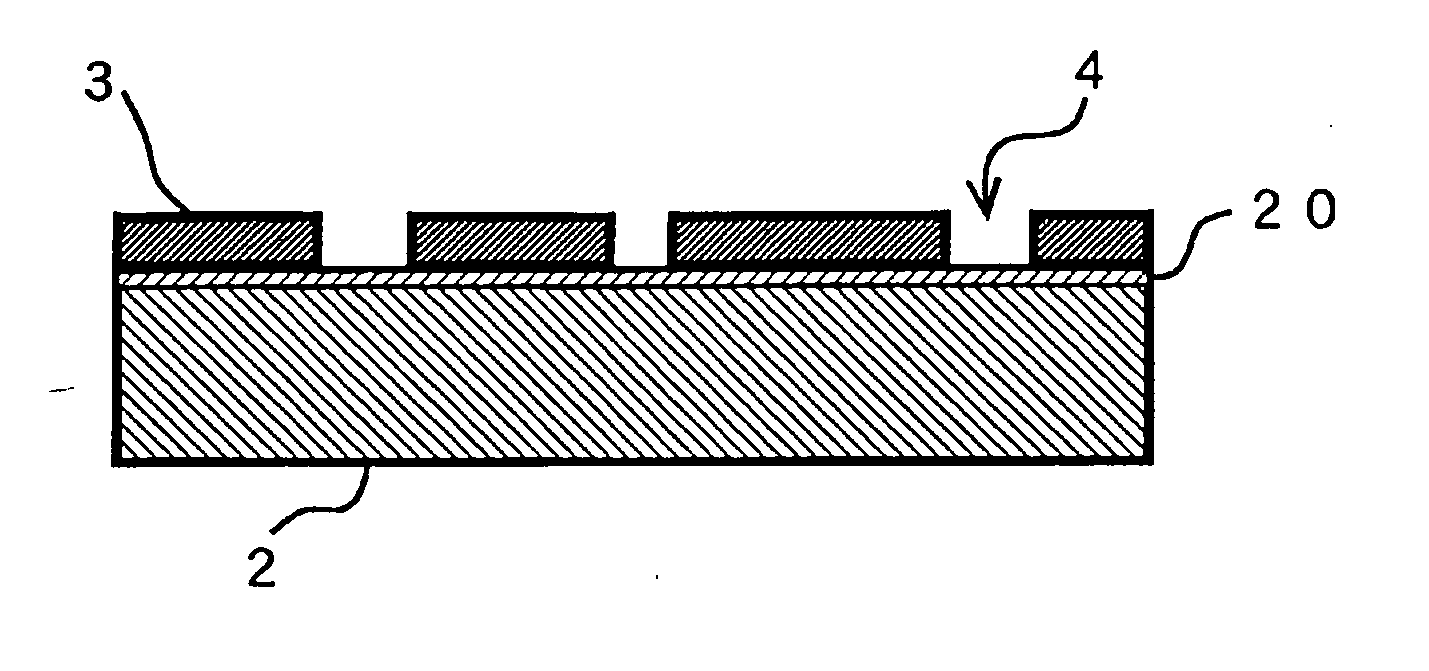
[0097] The high-melting-point metal layer 20 was formed on the surface of the dielectric layer 6 by using the dielectric-layer-provided copper foil 1A′ obtained as described above and the sputtering vapor deposition method. The high-melting-point metal layer 20 ...


PUM

PropertyMeasurementUnit
thicknessaaaaaaaaaa
particle diameter DIAaaaaaaaaaa

Abstract

To provide a dielectric-layer-provided copper foil or the like for extremely improving the product yield while making the most use of the increase effect of an electric capacity of a thin dielectric layer using the sputtering vapor deposition method. In the case of dielectric-layer-provided copper foils respectively having a dielectric layer on one side of a copper foil, the dielectric layer 6 is an inorganic-oxide sputter film having a thickness of 1.0 μm or less and formed on the one side of the copper foil in accordance with the sputtering vapor deposition method and the dielectric-layer-provided copper foils for respectively forming a capacitor layer, characterized in that a pit-like defective portion generated on the inorganic-oxide sputter film is sealed by polyimide resin are used.

Description

TECHNICAL FIELD [0001] The present invention relates to a copper foil provided with a dielectric layer for forming a capacitor layer, a copper clad laminate for forming the capacitor layer using the copper foil provided with the dielectric layer, and a method for manufacturing the copper foil provided with the dielectric layer for forming the capacitor layer. BACKGROUND ART [0002] It has been generalized in recent years to form a capacitor structure by a method same as the method for forming a circuit shape on an inner layer portion of a printed wiring board, particularly of a multilayer printed wiring board and use the capacitor structure as an embedded capacitor. By forming the capacitor structure on the inner layer portion of the multilayer printed wiring board, it has been possible to omit a capacitor set to the outer layer face, decrease an outer layer circuit in size and increase the outer layer circuit in density, decrease the number of surface-mounted components, and simplif...

Claims


Application Information

Patent Timeline
Patent Type & Authority Applications(United States)
IPC IPC(8): C23C14/00G01K5/66B32B15/20H01G4/33H05K1/16
CPCH01G4/33H05K1/162H05K2201/0154H05K2201/0179Y10T428/24926H05K2201/0355Y10T428/12903Y10T428/12514Y10T428/24917H05K2201/0195
Inventor YOKOTA, TOSHIKOMATSUNAGA, TETSUHIROTAKAHASHI, SUSUMUMATSUSHIMA, HIDEAKIYAMAMOTO, TAKUYADOBASHI, MAKOTO
Owner MITSUI MINING & SMELTING CO LTD
Learn More