Power supply antenna and power supply method
a technology of power supply antenna and power supply method, which is applied in the direction of individual energised antenna array, plasma technique, coating, etc., can solve the problem that film deposition cannot ensure the uniformity of film thickness throughout the surface of the wafer
- Summary
- Abstract
- Description
- Claims
- Application Information
AI Technical Summary
Benefits of technology
Problems solved by technology
Method used
Image
Examples
first embodiment
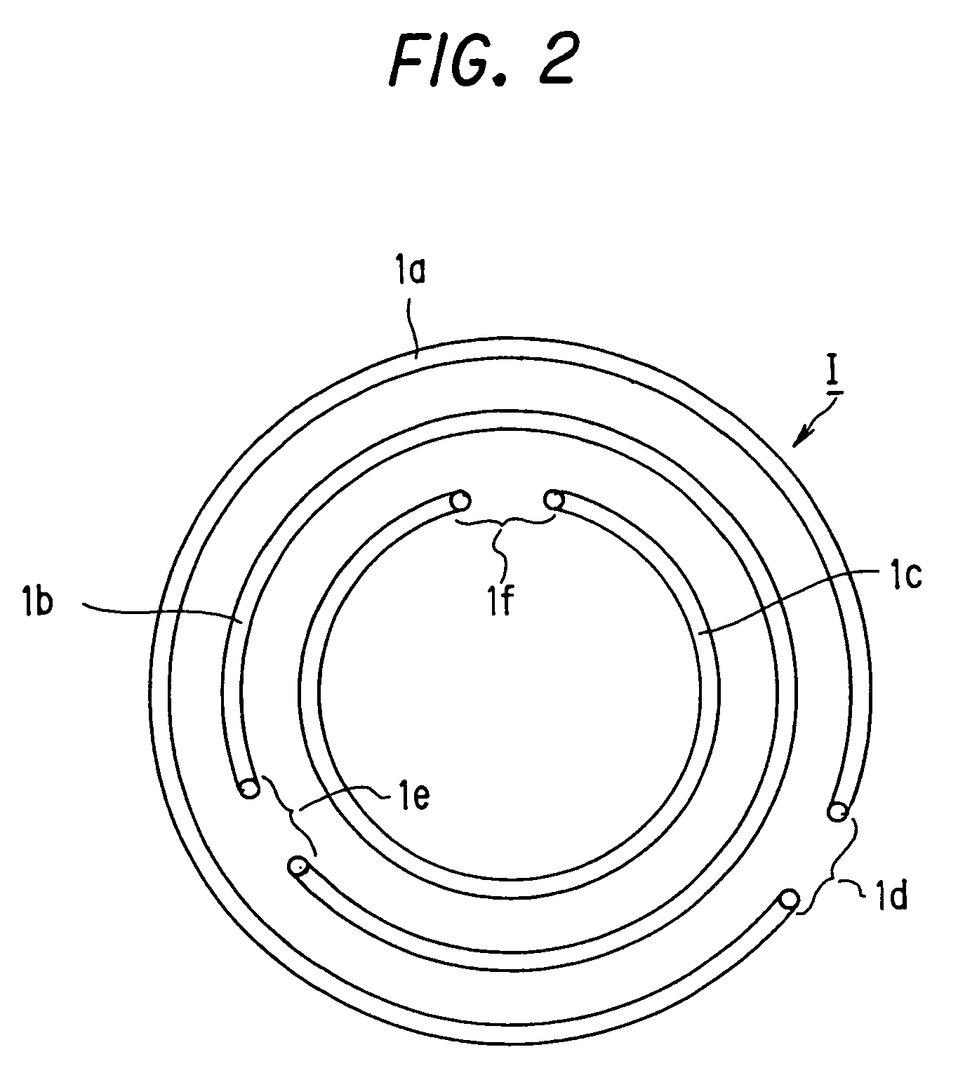
[0049]In the power supply antenna 01 comprising a concentric arrangement of the plural coils, 01a, 01b and 01c prepared by bending the plurality of conductors each into the form of an arc, the embodiment shown in FIG. 2 proposes that the disturbances in the electric field and the magnetic field at the power supply portions 01d, 01e and 01f be dispersed in the circumferential direction to minimize the influence of the Z-direction component Ez. FIG. 2 is a plan view showing a power supply antenna according to the present invention. As shown in the drawing, a power supply antenna I comprises a concentric arrangement of a plurality of coils, 1a, 1b and 1c, prepared by bending a plurality of (three in the drawing) conductors each into the form of an arc. Power supply portions 1d, 1e and 1f formed at opposite ends of the respective coils 1a, 1b and 1c so as to apply a high frequency voltage are configured to be located in different phases on the same plane. In the present embodiment, the ...
second embodiment
[0050]FIG. 3 is a plan view of a power supply antenna according to the present invention. As shown in the drawing, this power supply antenna II has a coil 1g on the innermost periphery which is a 2-turn coil. By this configuration, the inductances of respective coils 1a, 1b and 1g can be maximally approximated to each other, because these inductances correlate to the lengths of the respective coils 1a, 1b and 1g. Power supply portions 1d, 1e and 1h in the power supply antenna II are disposed, similar to the embodiment shown in FIG. 2, such that a phase difference of 120° exists between the adjacent power supply portions.
[0051]As described above, the power supply antennas I and II shown in FIGS. 2 and 3 are configured such that a certain phase difference is present between the adjacent power supply portions among the power supply portions (1d, 1e, 1f) and (1d, 1e, 1h) of the coils (1a, 1b, 1c) and (1a, 1b, 1g). Thus, the resulting electromagnetic wave can be uniformized. That is, the...
PUM
| Property | Measurement | Unit |
|---|---|---|
| frequency | aaaaa | aaaaa |
| frequency | aaaaa | aaaaa |
| electrical insulation | aaaaa | aaaaa |
Abstract
Description
Claims
Application Information


