Method of eliminating surface stress of silicon wafer
a technology of surface stress and silicon wafer, which is applied in the field of eliminating can solve the problems of increasing the cost of production, and increasing the leakage current. , to achieve the effect of reducing or eliminating the surface stress of silicon wafer, low cost and effective elimination
- Summary
- Abstract
- Description
- Claims
- Application Information
AI Technical Summary
Benefits of technology
Problems solved by technology
Method used
Image
Examples
example 1
The Effect of a Closed Anti-stress Groove on the Formation of Slip Lines
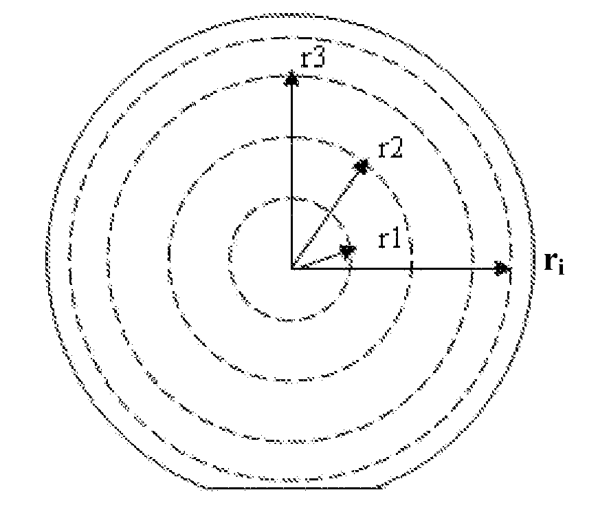
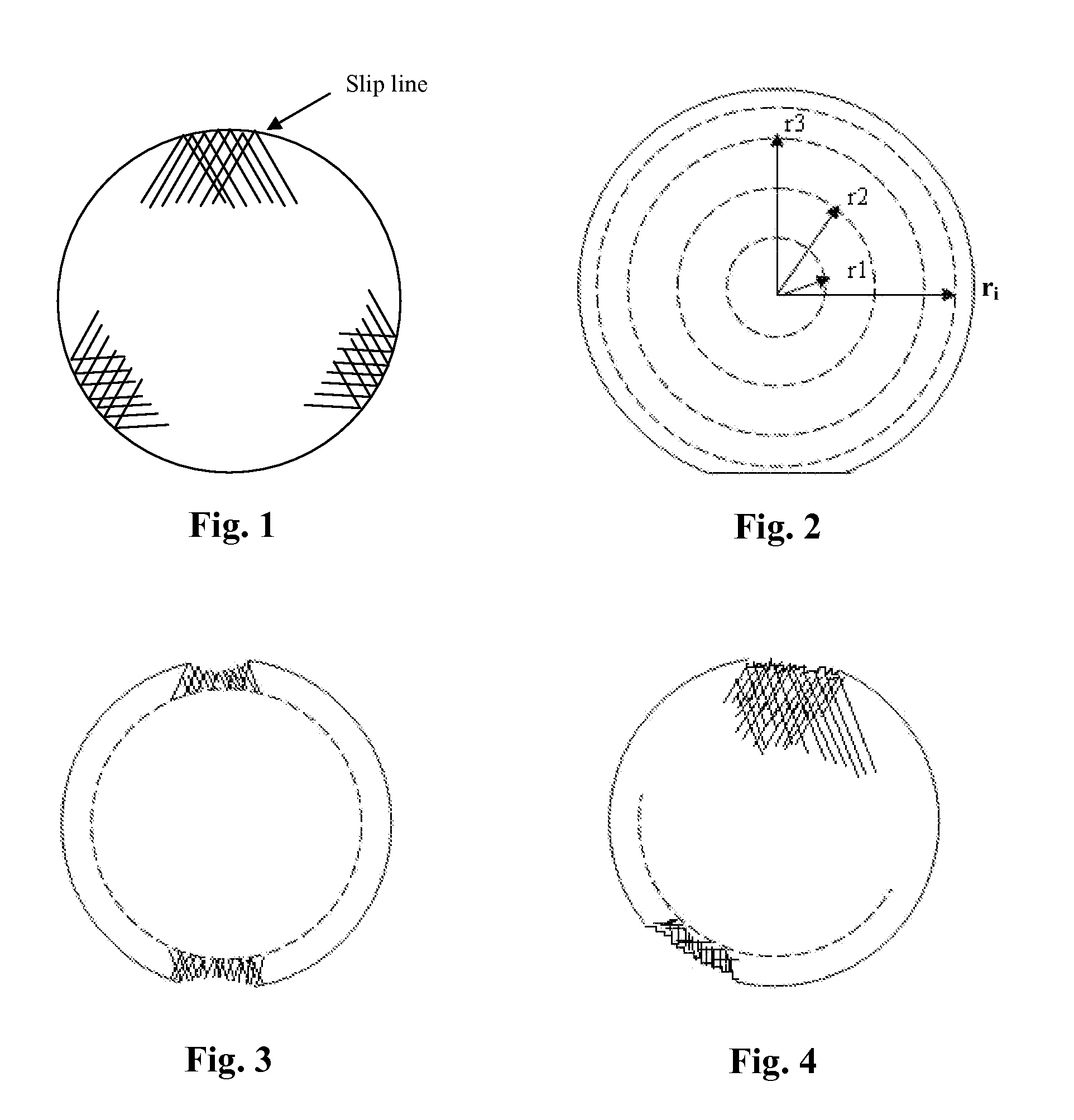
[0025]A silicon wafer with radius φ=35 mm and resistivity of 2-3×10³ Ω·cm was used in the experiment. The wafer was grinded and epitaxial growth was completed at 1200° C. Thereafter, a closed anti-stress groove was scored with a diamond blade at 3 mm from the edge of wafer. No slip lines were observed.
example 2
The Effect of Two Closed Anti-stress Grooves on the Formation of Slip Lines
[0026]Two uniform wafers, A and B, with radius φ=50 mm and resistivity 2-3×10³ Ω·cm were studied. Wafer A was scored with one groove at 3 mm from the edge of wafer, while wafer B was scored with two grooves: one at 3 mm from the edge of the wafer and the other at 12.5 mm from the center of the wafer. Thereafter, the wafers were grinded and epitaxial growth was completed at 1200° C. On wafer A, no slip lines were observed within 20 mm from edge, but there was a shallow slip line close to the wafer centre. On wafer B, no slip lines were observed.
example 3
The Effect of Several Closed Anti-stress Grooves on the Formation of Slip Lines
[0027]Two uniform wafers, A and B, with radius φ=100 mm and resistivity 2-3×10³Ω·cm were studied. Wafer A was scored with two grooves: one at 3 mm from the edge of wafer and the other at 37.5 mm from the center. Wafer B was scored with four grooves: one at 3 mm from the edge of wafer, and the other ones at 2.5 mm, 25 mm and 37.5 mm from the center, respectively. Thereafter, the wafers were grinded and epitaxial growth was completed at 1200° C. On wafer A, no slip lines were observed within 60 mm from edge, but there was a shallow slip line close to the wafer centre. On wafer B, no slip lines were observed.
PUM
| Property | Measurement | Unit |
|---|---|---|
| angle | aaaaa | aaaaa |
| groove angle | aaaaa | aaaaa |
| radius | aaaaa | aaaaa |
Abstract
Description
Claims
Application Information

