
Semiconductor mount substrate, semiconductor device and method of manufacturing semiconductor package

a semiconductor and mounting substrate technology, applied in the direction of applications, coatings, basic electric elements, etc., can solve the problems of reducing the wiring area on the wiring substrate, not an optimum solution, and the method is impractical, so as to prevent the occurrence of voids, improve the gate breakability, and reduce stress

Inactive Publication Date: 2009-04-28
PANASONIC CORP
View PDF12 Cites 2 Cited by
  • Summary
  • Abstract
  • Description
  • Claims
  • Application Information

AI Technical Summary

Benefits of technology

[0027]In view of the above-described problems, an object of the present invention is to provide a semiconductor mount substrate and a semiconductor realizable by the simplest method, having improved gate breakability, free from occurrence of voids and suitable for multiarray design, and a manufacturing method using the semiconductor mount substrate and the semiconductor device.

Problems solved by technology

However, this method has a problem that the encapsulation resin tends to flow mainly at a central position on each portion 13 to be resin encapsulated without sufficiently spreading out in the cavity of the encapsulation mold for forming the resin encapsulated portions 13 while flowing.
However, this method is impractical for the reason described below.
Disadvantageously, expansion of the plating portions results in a reduction in wiring area on the wiring substrate.
However, these methods are not an optimum solution to the above-described problem relating to gate break, the problem that voids (resin unfilled portions) occur at corners of a resin encapsulated portion, and other problems.
If the runner distance is increased, a load on the long runner acts on the narrow cross section of the gate, and a weak supporting structure results.
Therefore, there is a problem that when a force is applied in an unexpected direction to the runners by an erroneous operation or the like during transport of a plurality of semiconductor devices having resin encapsulated portions formed on the wiring substrate from the resin encapsulation step to the next gate break step for example, there is a possibility of the runners being broken in an unintended condition.

Method used


Image

  • Semiconductor mount substrate, semiconductor device and method of manufacturing semiconductor package
  • Semiconductor mount substrate, semiconductor device and method of manufacturing semiconductor package
  • Semiconductor mount substrate, semiconductor device and method of manufacturing semiconductor package

Examples


first embodiment

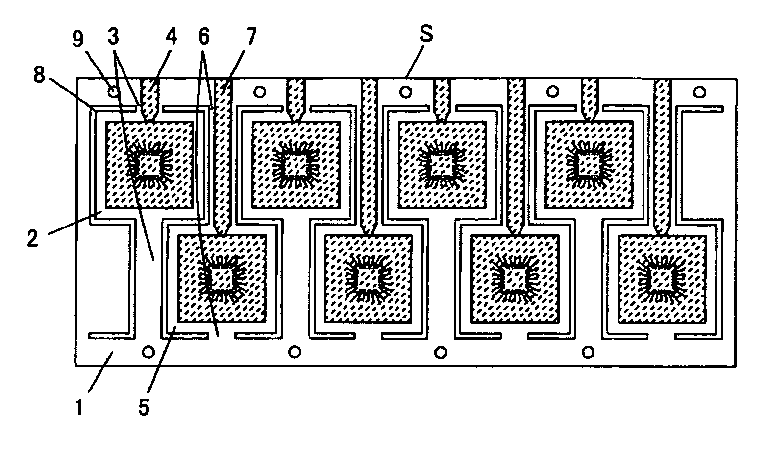
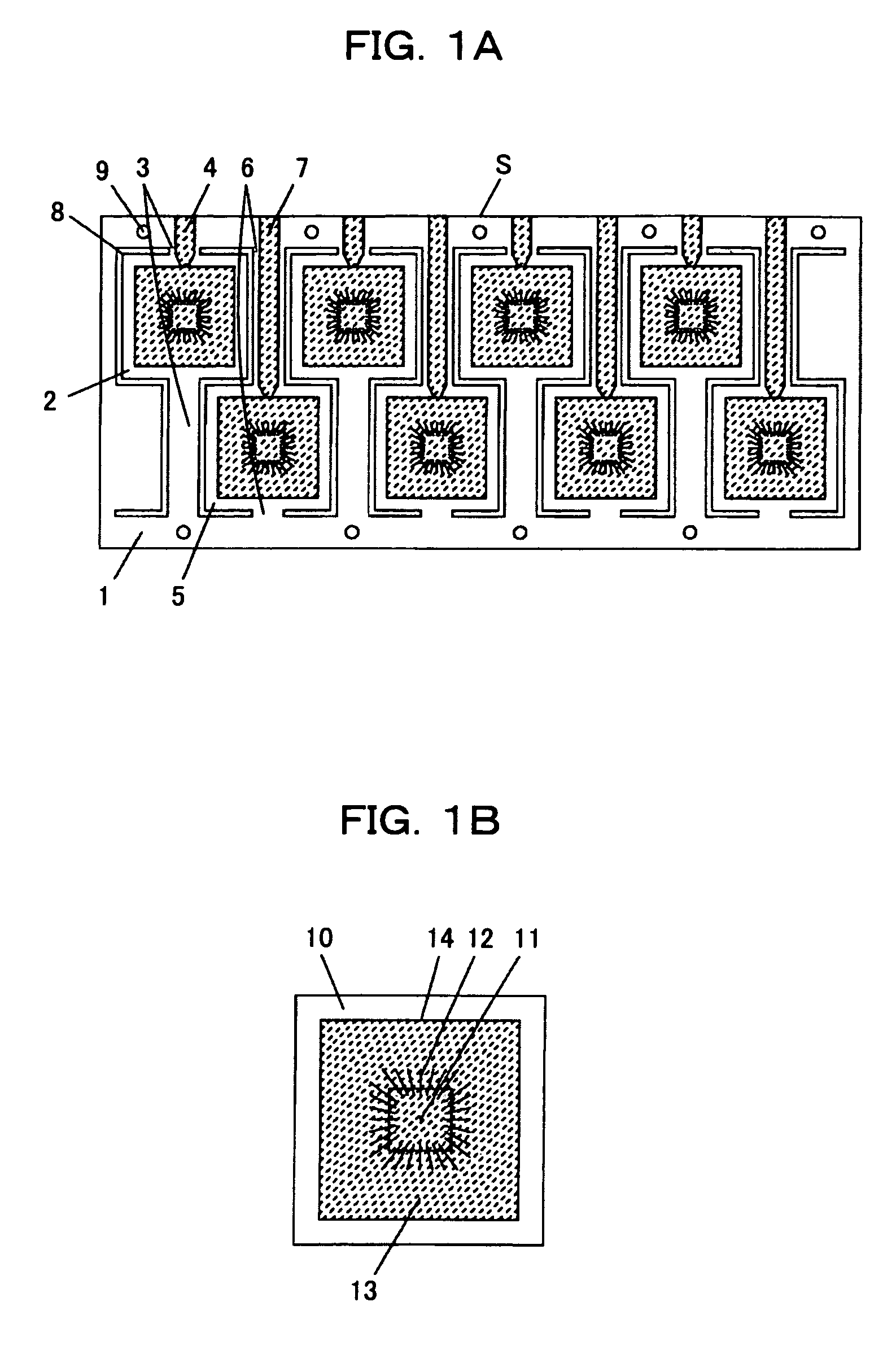
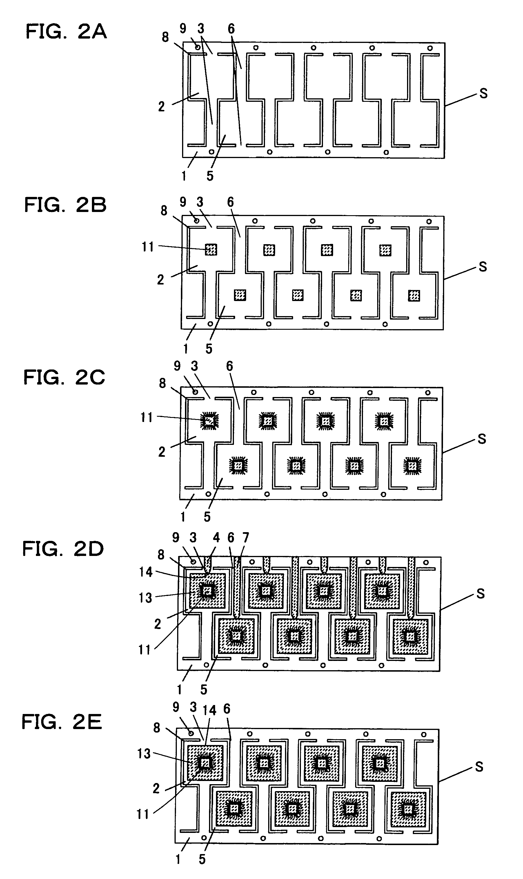
[0073]FIG. 1A shows an encapsulated state of a BGA package according to a first embodiment of the present invention. FIG. 1B shows a divided BGA package. FIGS. 2A to 2E show a process of manufacturing the BGA package using a semiconductor mount substrate according to the first embodiment of the present invention.

[0074]In FIGS. 1 and 2A to 2E, reference character S denotes a semiconductor mount substrate, reference numeral 1 a frame (connecting portion), reference numeral 2 a segment in a front row (a region divided in correspondence with each package), reference numeral 3 front-row tie bars, reference numeral 4 a runner to the front row, reference numeral 5 a segment in a rear row (a region divided in correspondence with each package), reference numeral 6 rear-row tie bars, reference numeral 7 a runner to the rear row, reference numeral 8 an opening, reference numeral 9 a positioning pin hole, reference numeral 10 a divided BGA package, reference numeral 11 a chip (semiconductor dev...

second embodiment

[0088]FIG. 3 shows an encapsulated state of a BGA package on a semiconductor mount substrate S in a second embodiment of the present invention. Referring to FIG. 3, the semiconductor mount substrate S is the same as that shown in FIG. 2A. The peripheral sides of segments 2 and 5 are formed parallel to the substrate peripheral edges of the frame 1. Chips 11 are mounted on the semiconductor mount areas of the segments 2 and 5, and resin encapsulated portions 13 in which the chips 11 are encapsulated are formed on the segments 2 and 5.

[0089]The sides of the external shape of each resin encapsulated portion 13 are inclined through 45 degrees from the peripheral sides of the segment 2 or 5. Each gate 14 is positioned at a center of one peripheral side of the segment 2 or 5 and at an apex of the resin encapsulated portion 13.

[0090]The above-described construction ensures that, at the time of gate break, i.e., when the runners 4 and 7 are cut off from the segments 2 and 5 and the resin enc...

third embodiment

[0095]FIG. 4 shows an encapsulated state of a BGA package on a semiconductor mount substrate S in a third embodiment of the present invention. Referring to FIG. 4, the semiconductor mount substrate S is basically the same as that shown in FIG. 2A. A point of difference therefrom is as described below.

[0096]That is, each of segments 2 and 5 has such a shape that its peripheral sides are inclined through 45 degrees from the substrate peripheral edges of the frame 1. On the segments 2 and 5 are formed resin encapsulated portions 13 in which chips 11 are encapsulated while being mounted on the semiconductor mount areas of the segments 2, as are those in the above-described embodiments.

[0097]The sides of the external shape of each resin encapsulated portion 13 are inclined through 45 degrees from the substrate peripheral edges of the frame 1 and are parallel to the peripheral sides of the segment 2 or 5. Each gate 14 is positioned at one apex of the segment 2 or 5 and at one apex of the ...


PUM

PropertyMeasurementUnit
angleaaaaaaaaaa
anglesaaaaaaaaaa
shapeaaaaaaaaaa

Abstract

Segments formed on a wiring substrate are arranged in a staggered array, and tie bars are provided between the segments.

Description

[0001]The present application claims priority to Japanese Patent Applications No. 2005-307914, filed Oct. 24, 2005, No. 2006-228510, filed Aug. 25, 2006 and No. 2006-228511, filed Aug. 25, 2006, the entire contents of which are expressly incorporated by reference.FIELD OF THE INVENTION[0002]The present invention relates to a semiconductor mount substrate, a semiconductor device and a method of manufacturing a semiconductor package and, more particularly, to a technique for a semiconductor package such as a ball grid array (BGA)BACKGROUND OF THE INVENTION[0003]In recent years, there has been a rapid progress in the development of semiconductor packages having an increased number of pins and a higher packaging density. In conventional semiconductor packages of this kind, lead-frame-type quad flat packages (QFPs) or the like have been in the mainstream but BGA packages using a substrate such as to have an advantage in terms of terminal density are now becoming mainstream.[0004]In gener...

Claims


Application Information

Patent Timeline
Patent Type & Authority Patents(United States)
IPC IPC(8): H01L23/495
CPCB29C45/14655H01L21/561H01L21/565H01L24/97B29C45/0025B29C45/2708B29C2045/0027H01L23/3121H01L2224/49171H01L2924/181H01L2924/00012
Inventor OCHI, TAKEO
Owner PANASONIC CORP
Learn More