Semiconductor circuit apparatus with voltage boost
a technology of circuit apparatus and capacitor, applied in the field of circuit apparatus with capacitor, can solve problems such as breakdown of operational circuit, incompatibility with cases in need, etc., and achieve the effect of suppressing an increase in the area
- Summary
- Abstract
- Description
- Claims
- Application Information
AI Technical Summary
Benefits of technology
Problems solved by technology
Method used
Image

Examples
first embodiment
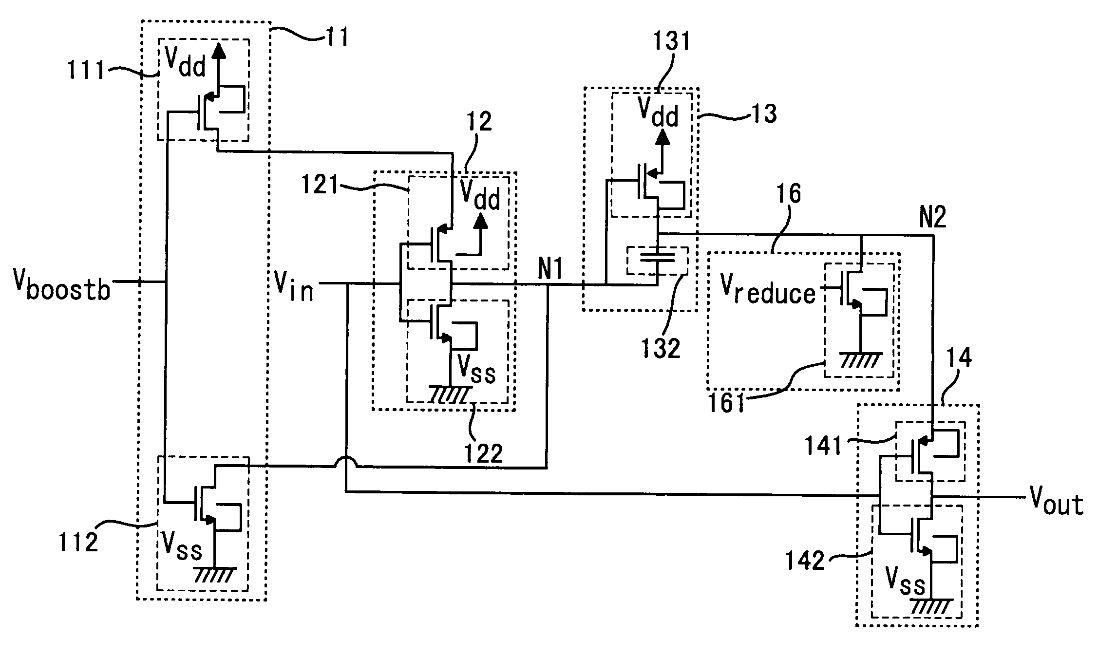
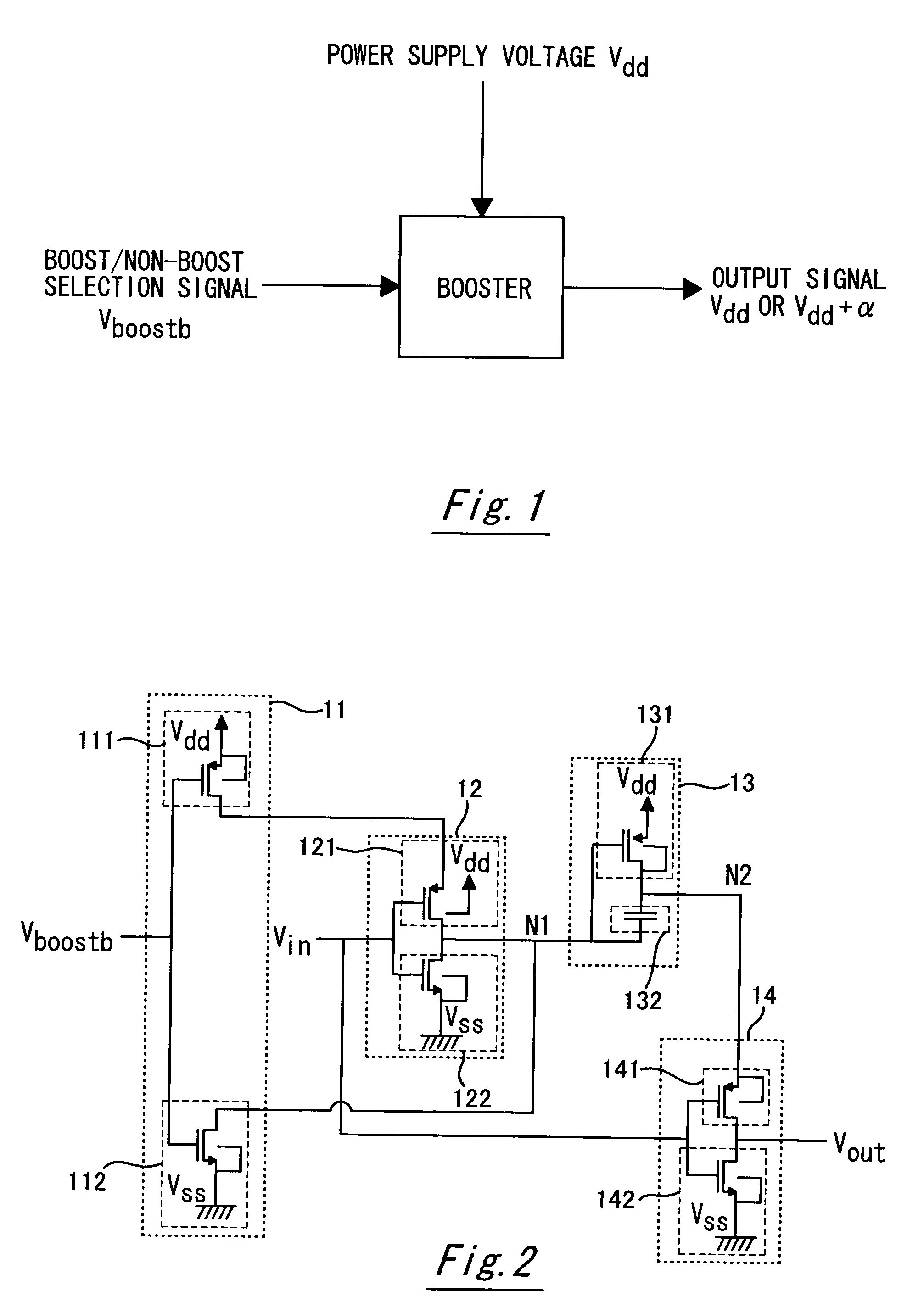
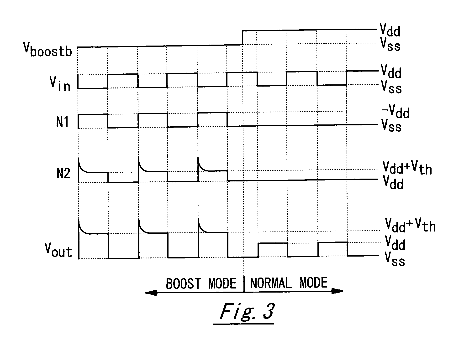
[0020]Embodiments of the present invention are described hereinafter in detail with reference to the drawings. FIG. 1 shows a pattern diagram of a semiconductor circuit apparatus according to a first embodiment of the invention. The semiconductor circuit apparatus of this embodiment has a booster to which a single power supply is connected and which selects one from a power supply voltage of the power supply and a converted voltage that is a higher than the power supply voltage according to a boost / non-boost selection signal Vboostb and outputs the selected voltage. The single power supply means a pair of a power supply Vdd on the high voltage side and a reference voltage Vss.
[0021]The use of the circuit according to this embodiment enables the control of the operation of a voltage converter that converts a power supply voltage and the selection of one from the power supply voltage and a converted voltage as the output of the voltage converter. It is thereby possible to produce a se...
second embodiment
[0052]FIG. 5 is a view showing the configuration of a semiconductor circuit apparatus 2 according to a second embodiment of the invention. The semiconductor circuit apparatus 2 of this embodiment includes a boost controller 11, a signal inverter 12, a booster 13, a signal output section 14, and a step-down controller 16. The same elements and operational principle as in the first embodiments are not described in detail herein.
[0053]The semiconductor circuit apparatus 2 of this embodiment further includes the step-down controller 16 in addition to the elements in the semiconductor circuit apparatus 1 of the first embodiment. The step-down controller 16 is composed of NMOS 161. A reduction / non-reduction selection signal Vreduce is input to the gate of the NMOS 161 in the step-down controller 16. Also in the step-down controller 16, the source of the NMOS 161 is connected to the reference voltage Vss, and the drain of the NMOS 161 is connected to the node N2, the drain of the PMOS 131 ...
third embodiment
[0060]A third embodiment applies the present invention to a voltage conversion signal processing unit as another aspect. FIG. 7 is a block diagram showing a voltage conversion signal processing unit according to this embodiment. The same elements and operational principle as in the first embodiments are not described in detail herein.
[0061]This embodiment uses the semiconductor circuit apparatus of the first embodiment as an amplitude converter 21. A boost / non-boost selection signal Vboostb which serves as a control signal of the amplitude converter 21 controls whether a CPU 24 in a control apparatus 30 boosts a signal or not. A voltage conversion apparatus 20 and the control apparatus 30 are placed to generate the boost / non-boost selection signal Vboostb as a control signal of the amplitude converter 21.
[0062]The voltage conversion apparatus 20 includes the amplitude converter 21, an A / D converter 22, and an A / D converter controller 23. The A / D converter controller 23 generates a s...
PUM
 Abstract
Description
Claims
Application Information
 - R&D
- Intellectual Property
- Life Sciences
- Materials
- Tech Scout
- Unparalleled Data Quality
- Higher Quality Content
- 60% Fewer Hallucinations
Browse by: Latest US Patents, China's latest patents, Technical Efficacy Thesaurus, Application Domain, Technology Topic, Popular Technical Reports.
© 2025 PatSnap. All rights reserved.Legal|Privacy policy|Modern Slavery Act Transparency Statement|Sitemap|About US| Contact US: help@patsnap.com