Semiconductor device having ferroelectric substance capacitor

a technology of ferroelectric substance and semiconductor device, which is applied in the direction of semiconductor devices, capacitors, electrical devices, etc., can solve the problems of high device integration, device easily receiving influence, and few escape routes of noise, and achieve high device reliability

Inactive Publication Date: 2009-05-12
ROHM CO LTD
View PDF13 Cites 7 Cited by
  • Summary
  • Abstract
  • Description
  • Claims
  • Application Information

AI Technical Summary

Benefits of technology

[0015]An another object of the invention is to provide a semiconductor device having a ferroelectric substance capacitor reducing influence of noise and being few in malfunctions.
[0030]According to such the construction, diffusion such as Pb or O2 from the ferroelectric substance thin film is depressed well, and it is possible to provide high device in reliability.

Problems solved by technology

Such the capacitor structure has large occupying area and it has been a large problem preventing michronization in LSI.
Further, there has been a problem that an escape route of noise is few so as to receive easily influence of noise as a device as shown in a explanation view of FIG. 9.
Thus, the conventional semiconductor device including the ferroelectric substance capacitor has large occupying area and it has been a large problem to prevent high integration of the device.
Further, the device easily receives influence of noise and it causes malfunction.

Method used


Image

  • Semiconductor device having ferroelectric substance capacitor
  • Semiconductor device having ferroelectric substance capacitor
  • Semiconductor device having ferroelectric substance capacitor

Examples


embodiment 1

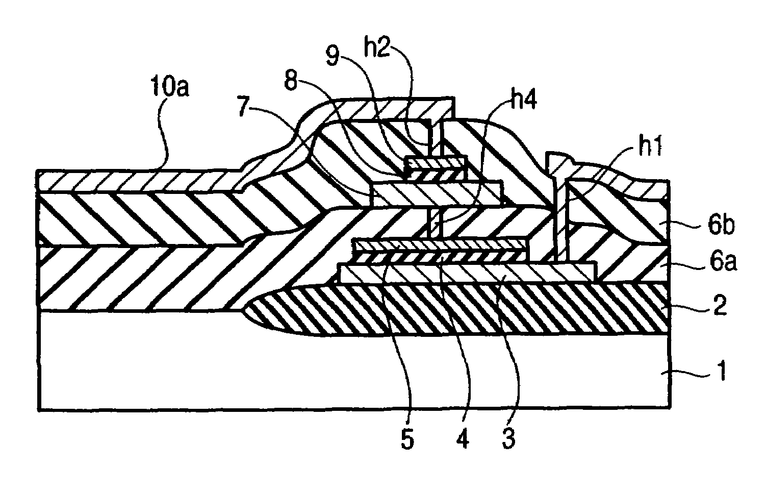
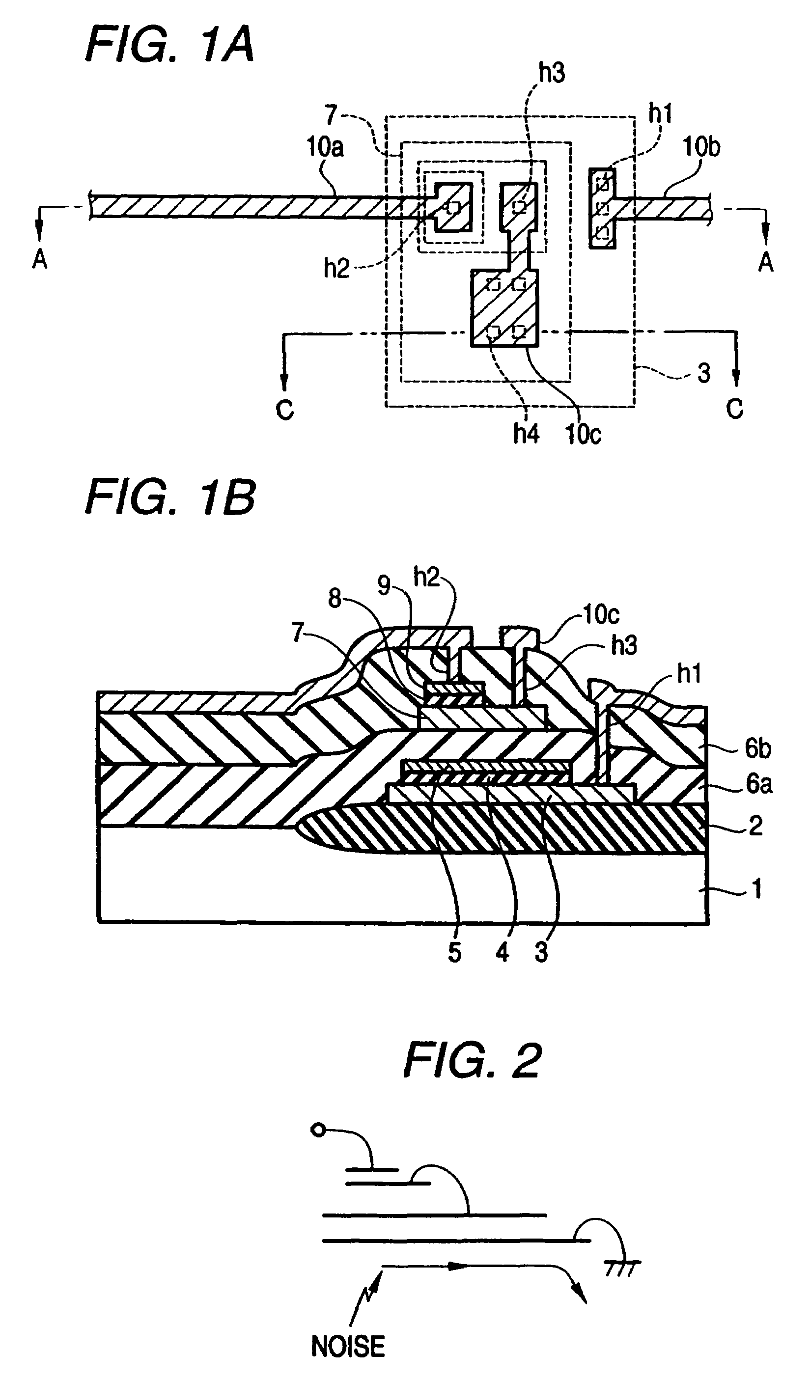
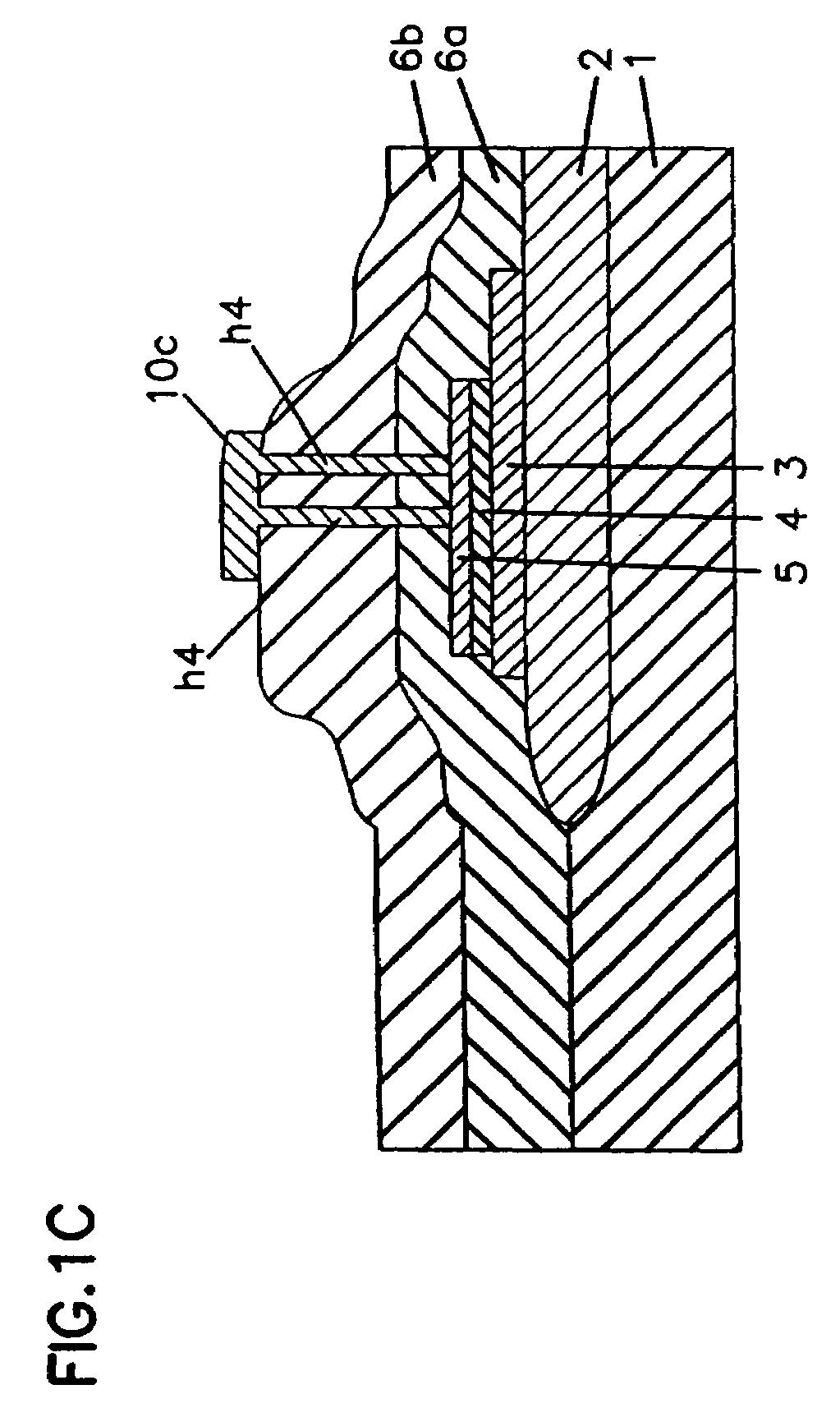
[0041]A semiconductor device having a PIP capacitor and a ferroelectric substance capacitor will be described for a first embodiment of the invention. The semiconductor device includes a first capacitor CPIP of a PIP capacitor formed on a surface of a semiconductor substrate and a second capacitor CFERO of a ferroelectric substance capacitor laminated on the first capacitor CPIP so as to connect thereto in series as shown in FIGS. 1A, a plane view, and 1B, a sectional view cut by A-A line.

[0042]That is, as shown in FIGS. 1A and 1B, the second capacitor CFERO of the ferroelectric substance capacitor is laminated on an element separating insulating film 2 formed on surface of a silicon substrate 1. The first capacitor and the second capacitor are connected in series through wiring pattern mutually connected through contact holes h3 to h4.

[0043]Here, the first capacitor is constructed by a first electrode 3 of a polysilicon layer formed on an element separating insulating film 2, a fir...

embodiment 2

[0064]Next, a second embodiment of the invention will be described with reference to FIGS. 4A and 4B. FIG. 4A is a plane view showing the semiconductor device of the second embodiment of the invention, and FIG. 4B is a sectional view cut by B-B line.

[0065]Although connection of the first capacitor and the second capacitor is performed by the wiring pattern of surface of the substrate through the contact hole formed at each electrode of each capacitor in the first embodiment, in the embodiment, the second electrode 5 positioning at the upper layer side of the first capacitor by plugs constructed by the fourth contact hole h4 formed at the first interlayer insulating film 6a formed on the upper layer of the first capacitor and the first electrode 7 of the second capacitor just on the second electrode 5 are connected after forming the first capacitor. Therefore, since electrodes are connected in the capacitor region, it is possible to design reduction of occupying area comparing the fi...

embodiment 3

[0068]Next, a third embodiment of the invention will be described with reference to FIGS. 5A and 5B. FIG. 5A is a plane view showing the semiconductor device of the third embodiment of the invention, and FIG. 5B is a sectional view cut by C-C line.

[0069]Although connection of the first capacitor and the second capacitor is performed through the contact hole formed at each electrode of each capacitor in the first embodiment, in the embodiment, the upper portion electrode of the first capacitor and the lower portion electrode of the second capacitor are constructed by a common electrode 11 of two-layer film of iridium and iridium oxide film. It is characterized that the capacitor insulating film 4 for the first capacitor is arranged at lower layer side of the common electrode 11 and the ferroelectric substance film 8 of PZT is arranged on the common electrode 11.

[0070]According to such the construction, since the upper portion electrode of the first capacitor and the lower part electr...


PUM


Abstract

The invention provides a semiconductor device having a ferroelectric substance capacitor small in the occupying area and large in capacitance and a semiconductor device having a ferroelectric substance capacitor reducing influence of noise and being few in malfunctions. The semiconductor device includes a first capacitor formed on a surface of a semiconductor substrate and a second capacitor of a ferroelectric substance capacitance laminated on the first capacitor so as to connect in series.

Description

[0001]This application is a Continuation of application Ser. No. 10 / 216109 filed Aug. 9, 2002, which application is incorporated herein by reference.BACKGROUND OF THE INVENTION[0002]The present invention relates to a semiconductor device having a ferroelectric substance capacitor, particularly to a structure for high integration.[0003]As high integration and michronization of semiconductor device advance, an occupying area of each part is decreased largely in LSI, and research for providing a semiconductor small and high in reliability is repeated.[0004]In the semiconductor device having the ferroelectric substance capacitor being researched now, a capacitor using an ordinary insulating layer for dielectric substance layer such as a capacitor, called PIP capacitor, having an insulating layer between polysilicon layers, or a capacitor, called MOS capacitor, formed sandwiching a silicon oxide film between a silicon layer and metal is used greatly at the same time in order to detect re...

Claims


Application Information

Patent Timeline
Patent Type & Authority Patents(United States)
IPC IPC(8): H01L29/94H01L27/04H01L21/02H01L21/822H01L21/8246H01L27/08H01L27/105
CPCH01L27/0805H01L28/55
Inventor FUJIMORI, YOSHIKAZU
Owner ROHM CO LTD
Why Eureka
Try Eureka