Methods for making display

a technology of light emitting elements and methods, applied in the field of light emitting image displays, can solve the problems of reducing the available space between light emitting elements of control lines and other circuits of backplanes, affecting the design of backplanes, and affecting the appearance of backplanes,

Inactive Publication Date: 2009-05-26
EASTMAN KODAK CO
View PDF23 Cites 48 Cited by
  • Summary
  • Abstract
  • Description
  • Claims
  • Application Information

AI Technical Summary

Problems solved by technology

These objectives can be difficult to achieve in a single display.
However, as the number of light emitting elements per unit area on a display increases, there is a decrease in available space between light emitting elements for the control lines and other circuits of the backplane.
Therefore, as the number of light emitting elements in the display increases, it becomes substantially more difficult to define a backplane on the same surface as the light emitting elements.
This approach can cause a variety of problems.
For example, inter-layer registration problems become difficult to solve in high-resolution displays.
This is because as the size of the light emitting elements is reduced it becomes increasingly difficult to align the circuits of the backplane with appropriate light emitting elements formed as another layer on the surface.
Further, the forming of multiple layers adds assembly steps and introduces the possibility of damaging the light emitting elements in the process of applying the backplane.
It will be appreciated that, even a single damaged light emitting element in a display can introduce an artifact in a displayed image that renders the display unsatisfactory for use by a consumer.
One barrier to the development of displays on flexible substrates is that it is difficult to maintain the integrity of the relationship between the backplane and the light emitting elements when the surface upon which they are formed can be deformed.
Further, there is a desire to form displays using non-flat surfaces such as curved or non-flat contours, fabrics, bottles, and the like as substrates, however, it is difficult to form backplanes using such surfaces.

Method used


Image

  • Methods for making display
  • Methods for making display
  • Methods for making display

Examples


Embodiment Construction

[0043]The present description is directed in particular to elements forming part of, or cooperating more directly with, apparatus in accordance with the invention. It is to be understood that elements not specifically shown or described may take various forms well known to those skilled in the art.

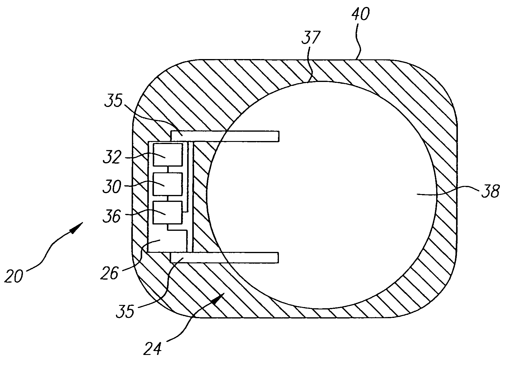
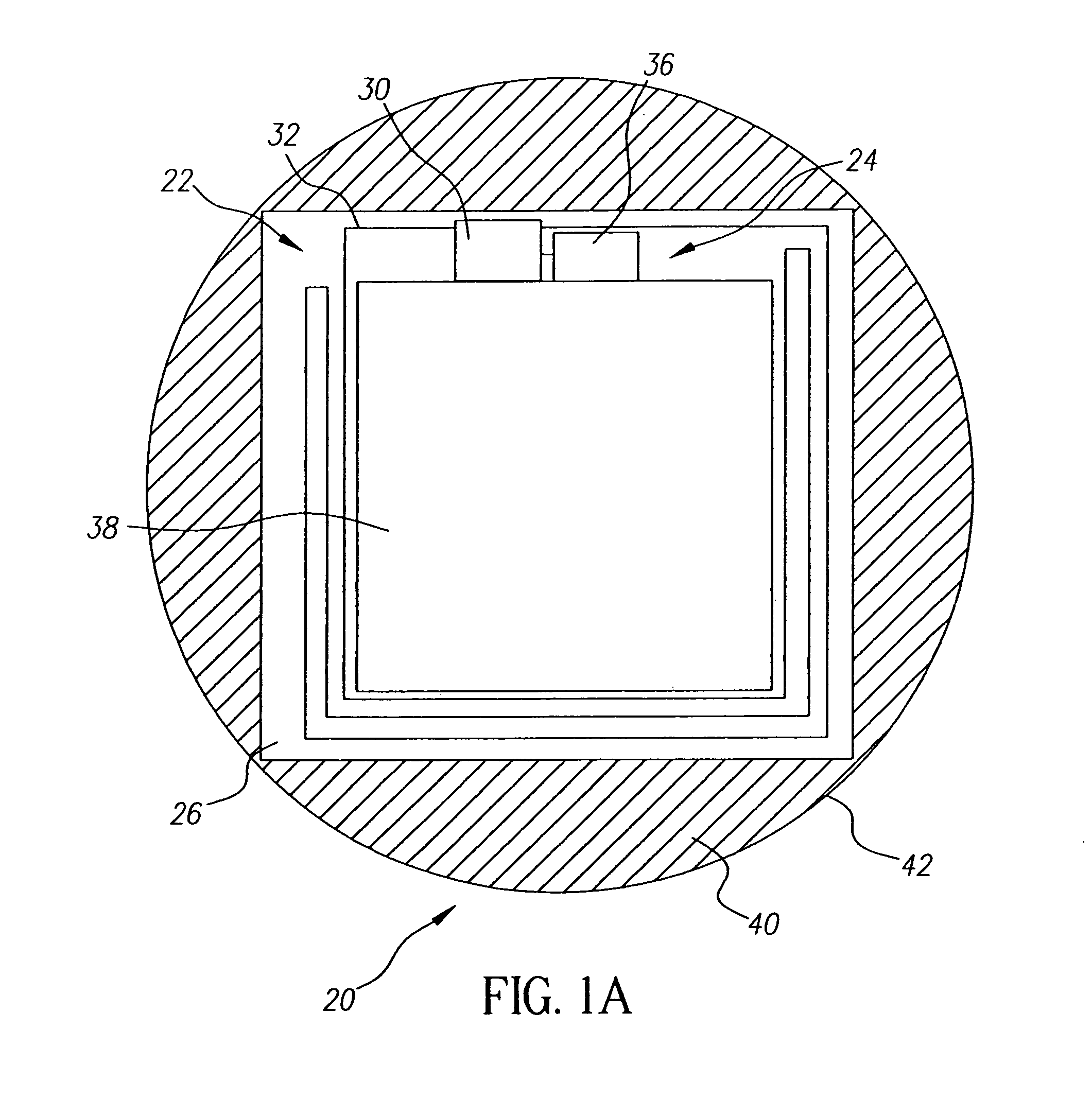
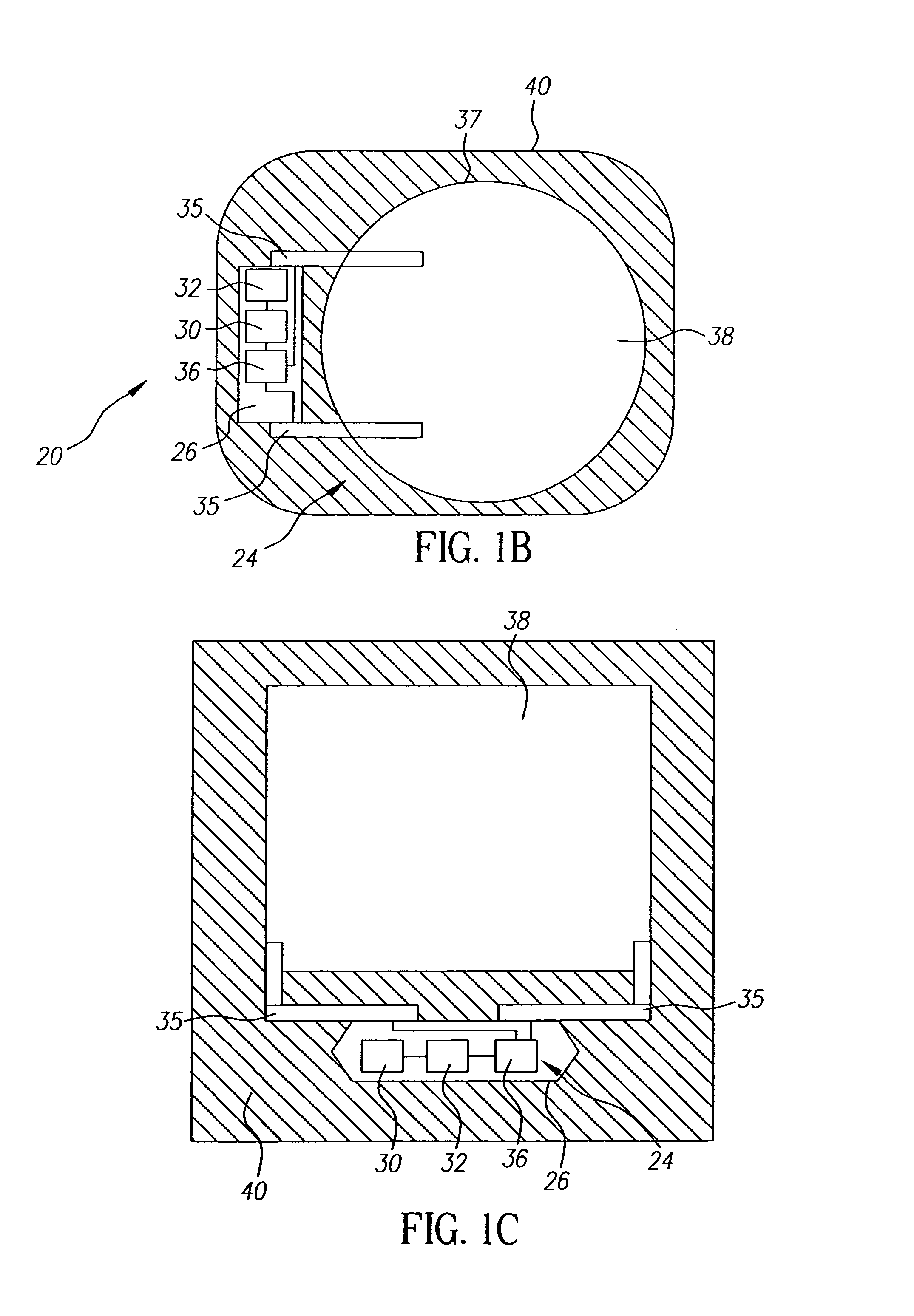
[0044]FIGS. 1A-1C show top cutaway views of one embodiment of an imaging element 20 of the present invention. In the embodiment of FIG. 1A, imaging element 20 comprises a wireless communication circuit 22, an illumination circuit 24 and a support 26. Wireless communication circuit 22 comprises, in this embodiment, a radio frequency receiver circuit 30 and an antenna 32. Antenna 32 is adapted to receive radio frequency signals and to provide the received signals to radio frequency receiver circuit 30. Radio frequency receiver circuit 30 is adapted to process the radio frequency signals received by antenna 32 and, in certain embodiments, to extract energy for operation from the radio frequen...


PUM


Abstract

Methods for forming a display using imaging elements are provided. In one method, a first surface is provided and imaging elements are provided on the first surface. The imaging elements are positionally aligned and a location order is determined for the imaging elements. Wherein the imaging elements each comprise: a wireless communication circuit adapted to detect a wireless communication signal and to generate a control signal; an illumination circuit having an illumination element, said illumination circuit being adapted so that the illumination element generates light at an intensity that is based upon the control signal. A body is provided containing the wireless communication circuit and the light source; wherein the body occupies a space that is less than about five cubic millimeters.

Description

CROSS-REFERENCE TO RELATED APPLICATIONS[0001]This application is related to U.S. Ser. No. 11 / 015,904 entitled DISPLAY, in the name of Kerr et al.; and U.S. Ser. No. 11 / 016,377 entitled IMAGING ELEMENT, in the name of Kerr et al., all filed concurrently herewith.[0002]Reference is made to commonly assigned, co-pending application U.S. Ser. No. 10 / 631,092, entitled A DIGITAL IMAGING ELEMENT in the name of Daniel Haas, filed on Jul. 31, 2003 and incorporated herein by reference.FIELD OF THE INVENTION[0003]The invention relates generally to the field of light emitting image displays, and in particular, methods for making displays.BACKGROUND OF THE INVENTION[0004]There is a general desire in the art of display technology to provide displays with high-resolution as measured in a number of imaging elements per unit area of the display surface and to provide displays that are low in cost. These objectives can be difficult to achieve in a single display. In particular, it is conventionally k...

Claims


Application Information

Patent Timeline
Patent Type & Authority Patents(United States)
IPC IPC(8): G09G3/36
CPCG09G3/001G09G3/06G09G3/3208G09G2310/02H01L33/20
Inventor KERR, ROGER S.TREDWELL, TIMOTHY J.
Owner EASTMAN KODAK CO
Why Eureka
Try Eureka