Light emitting device having a layer with a metal oxide and a benzoxazole derivative

a technology of metal oxide and benzoxazole, which is applied in the direction of discharge tube/lamp details, organic semiconductor devices, discharge tubes luminescnet screens, etc., can solve the problems of reducing the transmissivity of electrodes, difficulty in enhancing light extraction efficiency sufficiently, and increasing resistivity, so as to achieve the effect of enhancing light extraction efficiency and color purity of ligh

Inactive Publication Date: 2009-06-02
SEMICON ENERGY LAB CO LTD
View PDF30 Cites 25 Cited by
  • Summary
  • Abstract
  • Description
  • Claims
  • Application Information

AI Technical Summary

Benefits of technology

[0009]In view of the above-mentioned problems, it is an object of the present invention to provide a light-emitting device that is high in color purity of light and is high in light extraction efficiency, where sputtering is used to form an electrode on an electroluminescent layer without damage to a layer including an organic material.
[0016]According to the above-mentioned aspect of the present invention, even when a transparent conductive film formed by sputtering, for example, indium tin oxide (ITO), Indium Tin Oxide containing silicon (ITSO), or IZO (Indium Zinc Oxide) of indium oxide mixed with zinc oxide (ZnO) at 2 to 20% is used as the second electrode, sputter damage to a layer including an organic material of the electroluminescent layer can be suppressed, and then, the material for forming the second electrode has a wide range of choice. Further, in the present invention, the light extraction efficiency can be enhanced by extracting light from the second electrode side as compared with a case of extracting light from the first electrode side.
[0017]It is often the case that a spectrum of light obtained from a light-emitting element has a peak in a relatively wide wavelength range. Therefore, there is a problem that the color purity is inferior. Further, not only color purity but also reliability is required to be high as for characteristics of a light-emitting element. However, the present situation is spending a lot of time and cost to develop and obtain a light-emitting element that meets the both characteristics sufficiently. Consequently, in a light-emitting device according to the present invention, a plurality of light-emitting elements that have different wavelength ranges in emitting light and a color filter are used to extract only light in a specific wavelength range of light emitted from each of the light-emitting elements. According to the above-mentioned aspect of the present invention, even when a light-emitting element that has a relatively wide wavelength range is used, an unnecessary wavelength of light obtained from the light-emitting element is shielded by a color filter to enable extracting only a necessary wavelength range, hence it is easy to obtain a high color purity. Therefore, the electroluminescent material that is used for the light-emitting element is allowed to have a wide range of choice. In addition, the amount of light to be shielded by a color filter can be suppressed by selecting an electroluminescent material in accordance with a wavelength of light to be extracted as compared with a case of combining a light-emitting element that emits white light and a color filter, and the extraction efficiency can be enhanced.
[0019]As described above, according to the present invention, sputtering can be used to form an electrode on an electroluminescent layer without damaging a layer including an organic material, hence it is possible to provide a light-emitting device where a defect due to sputter damage is suppressed. Therefore, the material of the electrode to be formed on the electroluminescent layer is allowed to have a wide range of choice. In addition, a color purity of light can be easily enhanced by using a color filter, and a light extraction efficiency can be enhanced as compared to a case of combining a white light-emitting element and a color filter. Further, since it becomes possible to give priority to characteristics other than color purity, such as reliability, to some extent, the electroluminescent material is allowed to have a wide range of choice.

Problems solved by technology

However, in the former method of the above-mentioned two methods, it is difficult to enhance a light extraction efficiency sufficiently since transmissivity has a limit.
However, when sputtering is used to form a transparent conductive film typified by ITO (Indium Tin Oxide) on an electroluminescent layer, there is a problem that a layer including an organic material is subjected to damage (sputter damage) in the electroluminescent layer.
However, in this case, an electrode to be formed is reduced in transmissivity and is increased in resistivity, which is undesirable.
However, in the case of the former method, it is necessary to enhance the color purity of luminescence corresponding to each of R (red), G (green), and B (blue), and then spend a lot of cost and time to optimize an electroluminescent material and a device structure.
In the case of the latter method, light shielded by the color filter is wasted, and then, there is a problem that no high luminance can be obtained for the power consumption.

Method used


Image

  • Light emitting device having a layer with a metal oxide and a benzoxazole derivative
  • Light emitting device having a layer with a metal oxide and a benzoxazole derivative
  • Light emitting device having a layer with a metal oxide and a benzoxazole derivative

Examples


embodiment 1

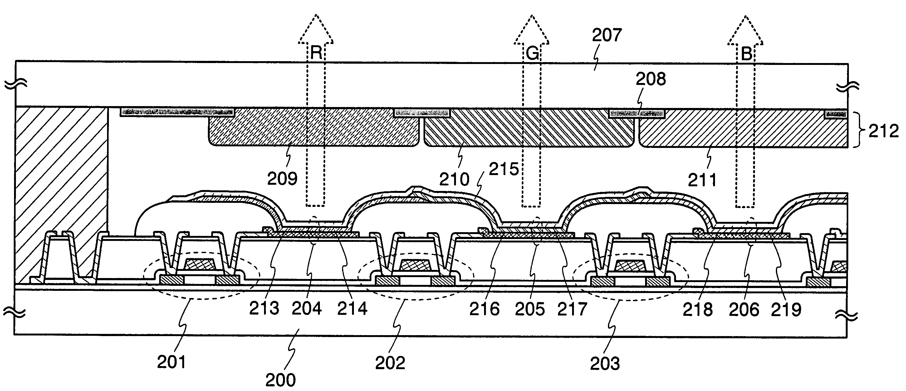
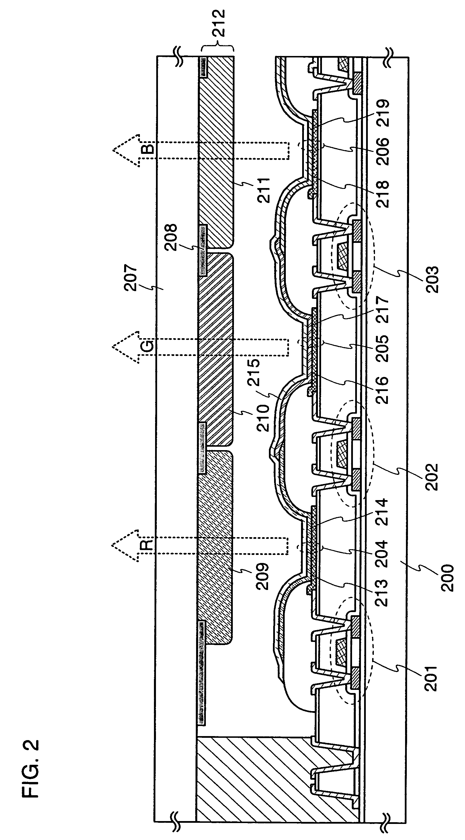
[0060]In the present embodiment, a form of how to lay out a light-emitting element and a coloring layer and shielding film of a color filter will be described.

[0061]FIG. 4A shows a top view of a pixel of a light-emitting device according to the present invention. However, FIG. 4A shows a state before sealing with a covering material, where reference numerals 401 to 403 denote light-emitting elements and reference numeral 404 denotes a wiring for controlling a supply of a signal or a power supply voltage to a pixel. Further, various interlayer films and a partition are omitted in the figure. In the present embodiment, the light-emitting element 401 is presumed to be formed in a pixel corresponding a red (R), the light-emitting element 402 is presumed to be formed in a pixel corresponding a green (G), and the light-emitting element 403 is presumed to be formed in a pixel corresponding a blue (B).

[0062]FIG. 4B then shows a state where the pixels shown in FIG. 4A are encapsulated with a...

embodiment 2

[0063]In the present embodiment, the mechanism of an improvement in color purity by a color filter will be described.

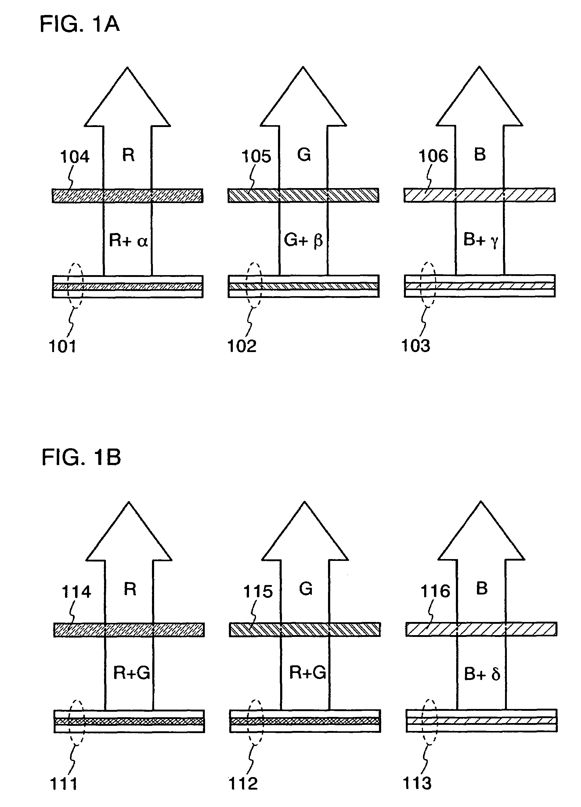
[0064]FIG. 5A shows a relationship between a wavelength of light and a transmissivity with respect to a coloring layer as an example. In FIG. 5A, the wavelength range that has shorter wavelengths than 600 nm is much lower in transmissivity than the wavelength range that has longer wavelengths than 600 nm.

[0065]Further, FIG. 5B shows a spectrum in the case of light in the wavelength range corresponding to a red, which is mixed with light in the wavelength range corresponding to a green. The spectrum shown in FIG. 5B has a small shoulder from 550 nm to 600 nm in addition to a peak in the wavelength range corresponding to the red including 700 nm. The light with this spectrum is low in purity of the red, and seems to be greenish red.

[0066]Then, by transmitting the light with the spectrum shown in FIG. 5B through the coloring layer that has the characteristics shown in FI...

embodiment 3

[0068]In the present embodiment, a specific example of a light-emitting element of a light-emitting device according to the present invention will be described.

[0069]With reference to FIG. 6A, a structure of a light-emitting element from which light in the wavelength range corresponding to a blue can be obtained will be described. The light-emitting element shown in FIG. 6A has, over a substrate 600, a first electrode 601, an electroluminescent layer 602 formed on the first electrode 601, and a second electrode 603 formed on the electroluminescent layer 602. In FIG. 6A, the first electrode 601 serves as a cathode and the second electrode 603 serves as an anode.

[0070]In the present invention, a metal, an alloy, an electrically conductive compound, and a mixture of these, which have a small work function and are generally used for a cathode of a light-emitting element, can be used to form the first electrode 601. Specifically, in addition to an alkali metal such as Li or Cs, an alkali...


PUM


Abstract

It is an object of the present invention to provide a light-emitting device that is high in color purity of light and is high in light extraction efficiency, where sputtering is used to form an electrode on an electroluminescent layer without damage to a layer including an organic material.The present invention provides a light-emitting device comprising a first light-emitting element that emits red light, a second light-emitting element that emits green light, a third light-emitting element that emits blue light, and a color filter, where the color filter comprises a first coloring layer that selectively transmits red light, a second coloring layer that selectively transmits green light, and a third coloring layer that selectively transmits blue light, the first to third light-emitting elements respectively correspond to the first to third coloring layers, wherein each of the first to third light-emitting elements has a first electrode, an electroluminescent layer formed on the first electrode, and a second electrode formed on the electroluminescent layer, and wherein the electroluminescent layer includes a layer in contact with the second electrode, and a metal oxide or a benzoxazole derivative is included in the layer in contact with the second electrode.

Description

BACKGROUND OF THE INVENTION[0001]1. Field of the Invention[0002]The present invention relates to a light-emitting device that has a light-emitting element in each pixel.[0003]2. Description of the Related Art[0004]A light-emitting element itself emits light with high visibility, needs no backlight that is required for a liquid crystal display device (LCD) to be suitable for reduction in thickness, and has no limit of viewing angle. Therefore, a light-emitting device using a light-emitting element has been attracting attention as an alternative display device to a CRT or an LCD, and has been putting into practical use. An OLED (Organic Light Emitting Diode) that is one of light-emitting elements has a layer including an electroluminescent material from which luminescence (electroluminescence) can be obtained by applying an electric field (hereinafter, referred to as an electroluminescent layer), an anode, and a cathode. By combining a hole injected from the anode and an electron inje...

Claims


Application Information

Patent Timeline
Patent Type & Authority Patents(United States)
IPC IPC(8): H01J63/04H01J1/62H01L27/32H01L51/50H01L51/52H05B33/00H05B33/02H05B33/14H05B33/26
CPCH01L27/3211H01L27/322H01L51/5092H01L51/5088H01L27/3244H01L27/3248H01L51/5052H01L2251/5315H01L51/5212H01L51/5228H01L51/5237H01L51/5284H10K59/35H10K59/38H10K59/123H10K59/12H10K50/155H10K50/165H10K50/17H10K50/171H10K50/814H10K50/824H10K50/846H10K50/8426H10K50/844H10K50/865H10K2102/3026H10K50/85H10K50/805H10K59/126H10K71/00H10K50/84H01L27/1218H01L27/1222H01L33/08H01L33/36H01L33/50H01L33/56H01L33/58
Inventor YAMAZAKI, SHUNPEISAKATA, JUNICHIROIKEDA, HISAONAKAMURA, YASUOSAITO, KEIKO
Owner SEMICON ENERGY LAB CO LTD
Why Eureka
Try Eureka