Process for producing semiconductor integrated circuit device

a technology of integrated circuits and semiconductors, applied in semiconductor devices, semiconductor/solid-state device details, electrical devices, etc., can solve the problems of parasitic capacitance that cannot be reduced between adjacent buried wiring lines, signal delay, and increase in resistance of via portions, so as to achieve high reliability of via connections and reduce parasitic capacitance

Inactive Publication Date: 2009-06-30
HITACHI LTD
View PDF11 Cites 210 Cited by
  • Summary
  • Abstract
  • Description
  • Claims
  • Application Information

AI Technical Summary

Benefits of technology

[0037]The present invention can provide a buried wiring portion in multiple layers having high reliable via connection and reduced parasitic capacitance due to an air-gap.

Problems solved by technology

This increases such parasitic capacitance to cause a signal delay.
From considerations conducted by the present inventors, it has been found that when the multi-layered buried wiring is formed using the technique described in the Patent, there may be problems of an increase in resistance of a via portion due to a defectively buried metal in the via portion, or parasitic capacitance that cannot be reduced between adjacent buried wiring lines because of metal films formed in the air-gap.

Method used


Image

  • Process for producing semiconductor integrated circuit device
  • Process for producing semiconductor integrated circuit device
  • Process for producing semiconductor integrated circuit device

Examples


example 1

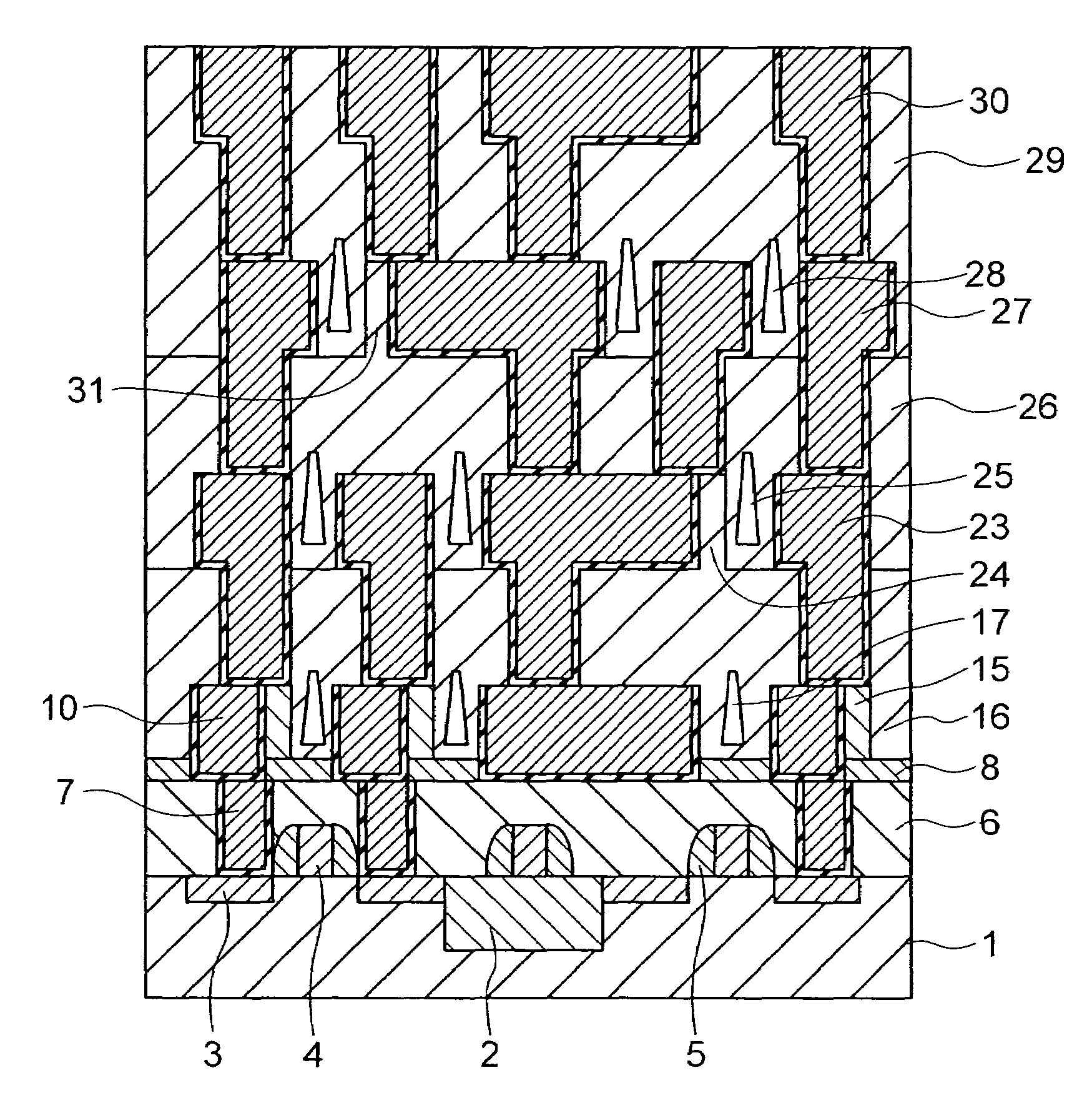
[0133]FIG. 1 is a cross sectional view of a substantial portion of a semiconductor device of an example 1 of the present invention.

[0134]The main surface of a semiconductor substrate 1 is divided into each of element regions by a field insulating film 2, and a diffusion layer 3 including a source region, drain region and the like is formed in each of the element regions. A gate electrode 4 composed of polycrystalline silicon is formed through a gate insulating film (not shown) between the regions of the source region and drain region 3 on the main surface of the semiconductor substrate 1, and lateral sides of the gate electrode 4 are covered with a side wall insulating film 5.

[0135]The diffusion layer 3 or the gate electrode 4 formed on the main surface of the semiconductor substrate 1 is connected to one end of a plug 7 through an interlayer insulating film 6, and the other end of the plug 7 is connected to a laminated single Damascene wiring portion 10 through the interlayer insul...

example 2

[0164]FIG. 15 is a cross sectional view of a substantial portion of a semiconductor device of an example 2 of the present invention.

[0165]The main surface of a semiconductor substrate 1 is divided into each of element regions by a field insulating film 2, and a diffusion layer 3 including a source region, drain region and the like is formed in each of the element regions. A gate electrode 4 composed of polycrystalline silicon is formed through a gate insulating film (not shown) between the regions of the source region and drain region 3 on the main surface of the semiconductor substrate 1, and lateral sides of the gate electrode 4 are covered with a side wall insulating film 5.

[0166]The diffusion layer 3 or the gate electrode 4 formed on the main surface of the semiconductor substrate 1 is connected to one end of a plug 7 through an interlayer insulating film 6, and the other end of the plug 7 is connected to a laminated single Damascene wiring portion 10 through the interlayer insu...

example 3

[0186]FIG. 20 is a cross sectional view of a substantial portion of a semiconductor device of an example 3 of the present invention.

[0187]The main surface of a semiconductor substrate 1 is divided into each of element regions by a field insulating film 2, and a diffusion layer 3 including a source region, drain region and the like is formed in each of the element regions. A gate electrode 4 composed of polycrystalline silicon is formed through a gate insulating film (not shown) between the regions of the source region and drain region 3 on the main surface of the semiconductor substrate 1, and lateral sides of the gate electrode 4 are covered with a side wall insulating film 5.

[0188]The diffusion layer 3 or the gate electrode 4 formed on the main surface of the semiconductor substrate 1 is connected to one end of a plug 7 through an interlayer insulating film 6, and the other end of the plug 7 is connected to a laminated single Damascene wiring portion 10 through the interlayer insu...


PUM


Abstract

An object of the present invention is to prevent formation of a badly situated via metal in a Damascene wiring portion in multiple layers having an air-gap structure. In the present invention, a via is completely separated from an air-gap 45 by forming an interlayer insulating film 44 having the air-gap 45 between adjacent Damascene wiring portions after forming a sacrifice film pillar 42 from a selectively removable insulating film in a formation region of a connection hole. The present invention can provide multiple-layered buried wiring in which a high reliable via connection and a reduced parasitic capacitance due to the air-gap are achieved.

Description

INCORPORATION BY REFERENCE[0001]The present application claims priority from Japanese application JP2005-331020 filed on Nov. 16, 2005, the content of which is hereby incorporated by reference into this application.BACKGROUND OF THE INVENTION[0002]1. Field of the Invention[0003]The present invention relates to a method for producing a semiconductor integrated circuit device, especially to a method for producing a semiconductor integrated circuit device having multi-layered buried wiring.[0004]2. Description of Related Art[0005]A structure of buried wiring is formed in a manner that wiring material is buried in an aperture for wiring such as a wiring groove or connection hole formed in an insulating film by wiring formation technologies as called Damascene Technologies (Single-Damascene Technology and Dual-Damascene Technology).[0006]Recently, an increase in integration of the semiconductor integrated circuit device has reduced a clearance between such buried wiring lines. This incre...

Claims


Application Information

Patent Timeline
Patent Type & Authority Patents(United States)
IPC IPC(8): H01L21/4763
CPCH01L21/76802H01L21/76807H01L21/76814H01L21/7682H01L21/76831H01L21/76834H01L23/5222H01L23/53223H01L23/53238H01L23/53252H01L23/53266H01L23/53295H01L21/76849H01L2221/1026H01L2924/0002H01L2924/00
Inventor HAYASHI, HIROYUKIOSHIMA, TAKAYUKIAOKI, HIDEO
Owner HITACHI LTD
Why Eureka
Try Eureka