Versatile system for integrated sense transistor

a transistor and integrated sense technology, applied in the field of semiconductor circuitry, can solve the problems of inability to fully realize the effect of sensing, low degree of accuracy of such approximation, and relatively high cost of components, and achieve the effect of convenient implementation

Active Publication Date: 2009-06-30
NAT SEMICON CORP
View PDF7 Cites 29 Cited by
  • Summary
  • Abstract
  • Description
  • Claims
  • Application Information

AI Technical Summary

Benefits of technology

[0009]The present invention provides a versatile system, comprising various constructs and methods, for providing a sense transistor structure—particularly a sense FET—optimally matched with an associated power transistor. The system of the present invention integrates one or more sense transistor structures within the architecture of a power transistor. The sense transistor architecture of the present invention shares

Problems solved by technology

Generally, most designs seek to minimize the number of “power” transistors—as such components are relatively expensive and cumbersome, when compared to their low-voltage counterparts.
In the past, the level of accuracy with which such sensing approximations were made was—in some cases—marginal.
At the time, however, system using such approaches may not have needed highly accurate sensing.
Even where a sense FET is fabricated around the immediate perimeter of a power FET, only a limited level of matching or accuracy can be attained.
Fabrication and processing variations between the transistor structures in the center of a large power FET and a sense FE

Method used


Image

  • Versatile system for integrated sense transistor
  • Versatile system for integrated sense transistor
  • Versatile system for integrated sense transistor

Examples


Embodiment Construction

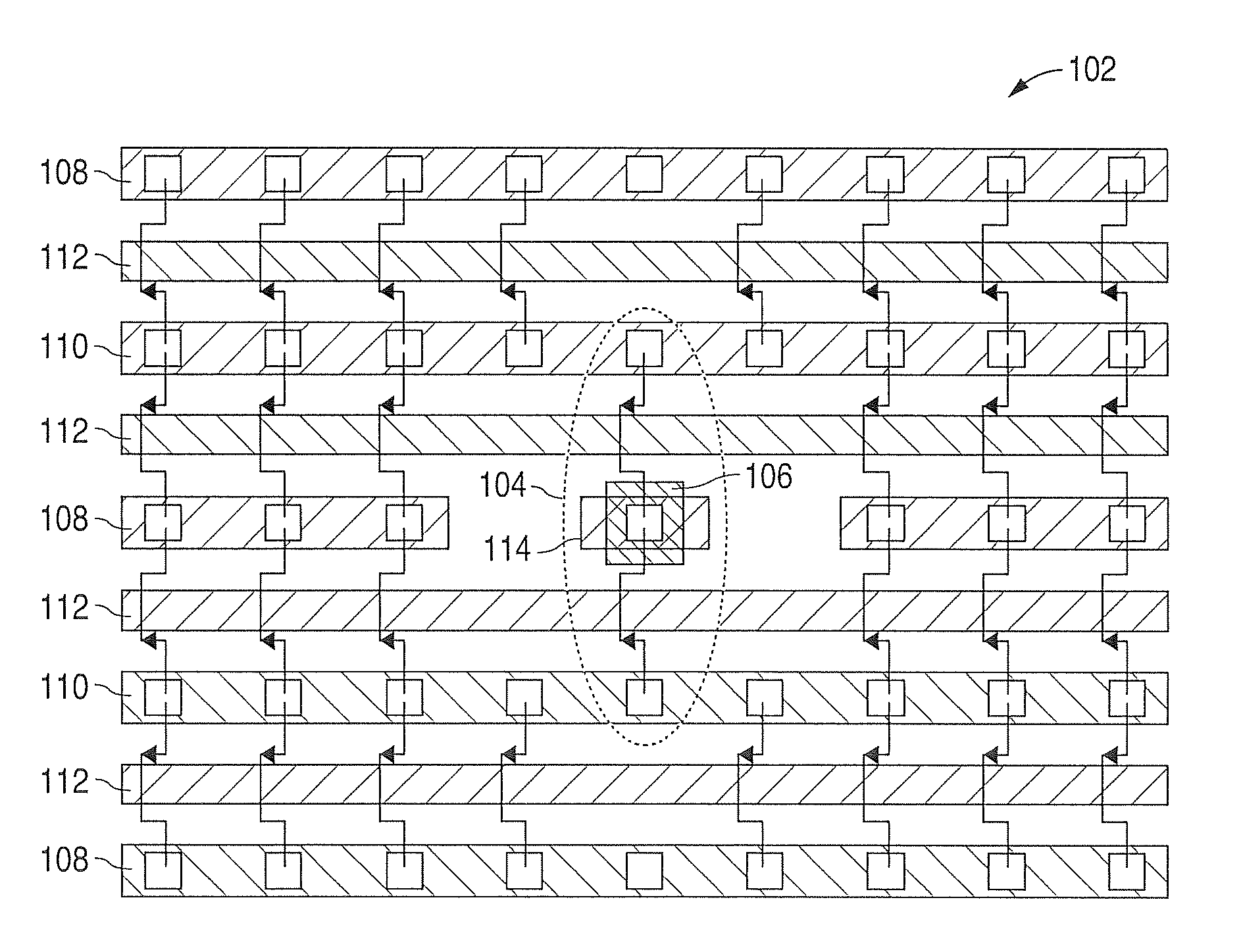
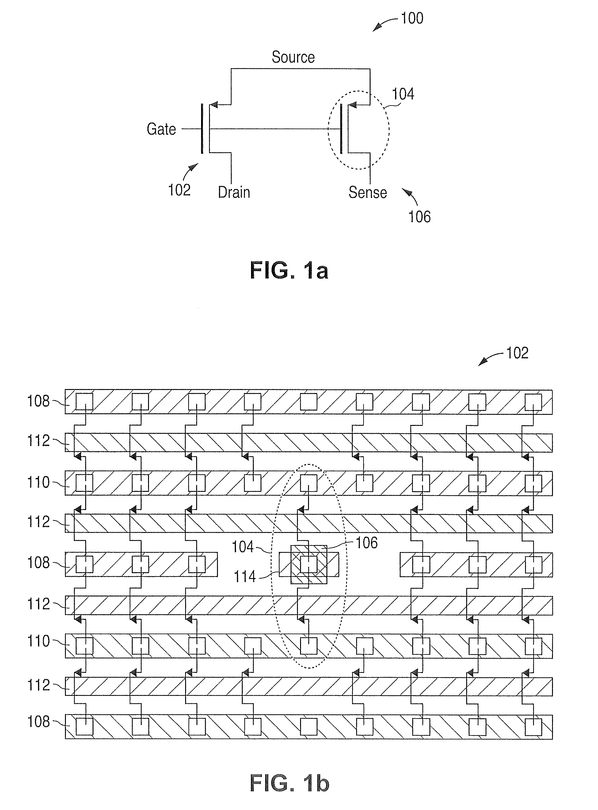
[0016]While the making and using of various embodiments of the present invention are discussed in detail below, it should be appreciated that the present invention provides many applicable inventive concepts, which can be embodied in a wide variety of specific contexts. The present invention is hereafter illustratively described in conjunction with the design and operation of sense transistor structures—particularly sense FETs (field effect transistors)—utilized in conjunction with certain power transistors—particularly power FETs. Although described in relation to such constructs and applications, the teachings and embodiments of the present invention may be beneficially implemented with a variety of semiconductor devices and technologies. The specific embodiments discussed herein are, therefore, merely demonstrative of specific ways to make and use the invention and do not limit the scope of the invention.

[0017]The present invention provides a versatile system, comprising various ...


PUM


Abstract

The present invention provides a versatile system for producing sense transistors having optimized thermal and parametric matching with an associated power transistor. A power transistor is formed, having a plurality of alternating source and drain structures, with a plurality of gate structures interposed there between. At a desired location within the power transistor—which may be in a central location, or symmetrically distributed—one or more sense transistors are formed from an isolated portion of either a drain or source structure.

Description

TECHNICAL FIELD OF THE INVENTION[0001]The present invention relates generally to semiconductor circuitry and, more particularly, to a system for providing highly accurate sense transistor circuitry.BACKGROUND OF THE INVENTION[0002]In a number of modern electronics systems, various transistor structures are designed to operate at, and withstand, different voltage and current levels. For example, numerous designs commonly utilize high-voltage “power” transistors in conjunction with low-voltage transistors. Generally, most designs seek to minimize the number of “power” transistors—as such components are relatively expensive and cumbersome, when compared to their low-voltage counterparts. To this end, and in order to successfully interface higher voltage transistors to their low-voltage counterparts, many designs pair high power transistor structures with some configuration of lower power sensing transistors.[0003]Commonly, sensing transistors are configured in a manner that divides or ...

Claims


Application Information

Patent Timeline
IPC IPC(8): H01L29/788
CPCH01L21/823418H01L27/088
Inventor RANUCCI, PAULLABICANE, ROBERT
Owner NAT SEMICON CORP
Why Eureka
Try Eureka