Phase-locked loop circuit having correction for active filter offset

a phase-locked loop circuit and active filter technology, applied in the direction of digital transmission, pulse automatic control, electrical equipment, etc., can solve the problems of serial data stream being instantly cut off in reproduction, the lock point of signal reproduction tends to deviate, and the influence of various characteristics of the pll circuit, etc., to increase the measurement resolution of offset correction and correction resolution, and high reliability

a phase-locked loop circuit and active filter technology, applied in the direction of digital transmission, pulse automatic control, electrical equipment, etc., can solve the problems of serial data stream being instantly cut off in reproduction, the lock point of signal reproduction tends to deviate, and the influence of various characteristics of the pll circuit, etc., to increase the measurement resolution of offset correction and correction resolution, and high reliability

US7554412B2Active Publication Date: 2009-06-30TEXAS INSTR INC

Image

  • Phase-locked loop circuit having correction for active filter offset
  • Phase-locked loop circuit having correction for active filter offset
  • Phase-locked loop circuit having correction for active filter offset

Examples


Embodiment Construction

[0032]With the phase-locked loop circuit of the present invention, due to the aforementioned configuration and operation, the offset of the analog (especially the active type) loop filter is automatically corrected, the stability and precision of the locked clock or locked frequency are improved, and the reliability of the PLL function can be improved.

[0033]Optimum Scheme for Embodiment of the Invention

[0034]In the following, an explanation will be given regarding a preferred embodiment of the present invention with reference to the annexed drawings.

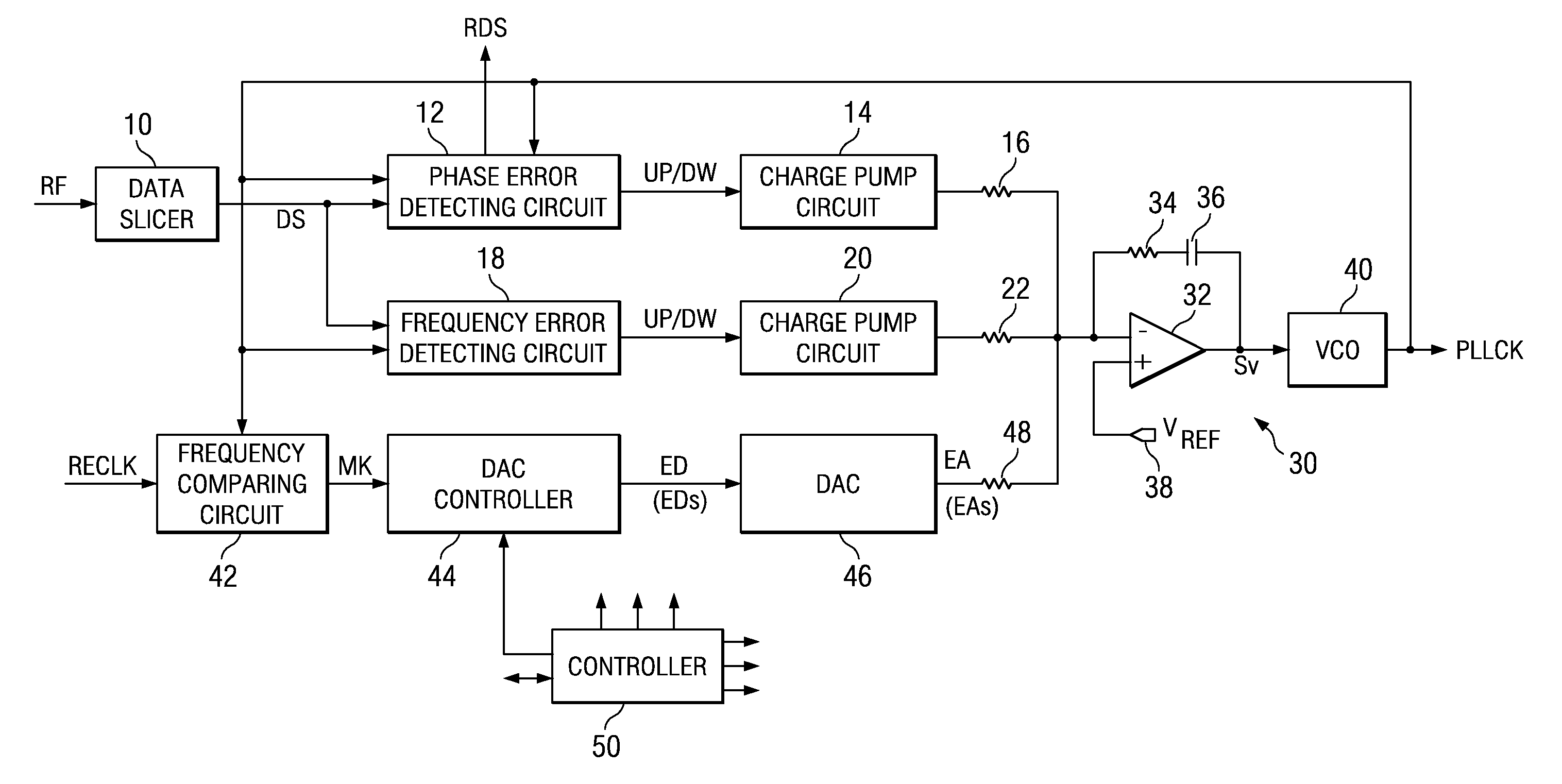
[0035]FIG. 1 is a diagram illustrating the configuration of the PLL circuit in an embodiment of the present invention. This PLL circuit is formed as a clock extraction type digital PLL circuit having an analog loop filter, and, for example, it can be applied to clock data recovery (CDR) during reproduction of optical disks, the as CDs and DVDs.

[0036]In data slicer 10 of the input section, for example, the reproduction RF signal (serial d...


PUM


Abstract

A phase locked loop (PLL) circuit automatically corrects the offset of the analog (especially active type) loop filter to improve the stability and precision of the locked clock or frequency signals. In addition to the general PLL circuit configuration having active type loop filter (30), the PLL circuit also has a frequency comparing circuit (42), a DAC controller (44) and a DAC (digital-to-analog converter) (46). In an offset measurement mode, the outputs of phase error detecting circuit (12, 14) and frequency error detecting circuit (18, 20) are cut, respectively, to establish locking in offset measurement locked loop (42, 44, 45, 30, 40). In this case, offset correction code (EDs) are identified and held. In normal mode, DAC controller (44) has offset correction code (ED) input to DAC (46), and DAC (46) sends offset correction signal (EAs) to loop filter (30).

Description

[0001]The present invention relates to a phase-locked loop (PLL) circuit; and, in particular, to a PLL circuit that contains an analog loop filter.BACKGROUND OF THE INVENTION[0002]FIG. 5 illustrates the basic layout of a digital PLL circuit that contains an analog loop filter. This PLL circuit comprises a clock signal input / output type phase comparing circuit 100, an analog loop filter 102, and an analog input / output type voltage-controlled oscillator (VCO) 104. An input clock signal INCK and the feedback clock signal PLLCK output from VCO 104 are input to phase comparing circuit 100, which outputs analog phase error signal Φer representing the phase error of the two clock signals INCK, PLLCK. Loop filter 102 is a low-pass filter, which integrates phase error signal Φer output from phase comparing circuit 100. The output voltage of loop filter 102 is a control voltage Sv, which is input to VCO 104. VCO 104 oscillates and outputs variable frequency clock PLLCK whose frequency corresp...

Claims


Application Information

Patent Timeline
30 Jun 2009
Publication
US7554412B2
IPC
H03L7/087; H03L7/093
CPC
H03L7/087; H03L7/10; H04L7/0337; H03L7/113
Inventors
KOJIMA, HIROAKI; MATSUSHIMA, ISAMU