Optical device wafer, and optical device chip and method for manufacturing the same

a technology of optical devices and optical wafers, applied in the direction of optical elements, instruments, semiconductor lasers, etc., can solve the problems of long lamination layer time, device damage, and limited measures, so as to prevent electrostatic destruction and improve reliability.

Inactive Publication Date: 2009-07-28
SEIKO EPSON CORP
View PDF15 Cites 0 Cited by
  • Summary
  • Abstract
  • Description
  • Claims
  • Application Information

AI Technical Summary

Benefits of technology

[0007]In accordance with an advantage of some aspects of the invention, electrostatic destruction can be prevented and reliability can be improved in optical device wafers, and optical device chips and methods for manufacturing the same.
[0009]In the optical device wafer, the connecting section serves as a refuge for a current. In other words, upon application of a voltage that may cause electrostatic destruction at an optical section (to be described below) in each of the chip regions, a current is circulated and distributed in the connecting section and the electrodes of the other chip regions. By this, electrostatic destruction of the optical section can be prevented in an optical device chip manufacturing process, such that, by the optical device wafer described above, the reliability can be improved.

Problems solved by technology

An optical device such as a surface-emitting type semiconductor laser itself has a low electrostatic breakdown voltage, such that the device may be damaged by static electricity caused by a machine or an operator in a mounting process.
A variety of measures are usually implemented in a mounting process to remove static electricity, but these measures have limitations.
In this case, it may take a long time for laminating layers to form a desired capacitance device as the insulating films and metal films are laminated.

Method used


Image

  • Optical device wafer, and optical device chip and method for manufacturing the same
  • Optical device wafer, and optical device chip and method for manufacturing the same
  • Optical device wafer, and optical device chip and method for manufacturing the same

Examples


Embodiment Construction

[0029]Preferred embodiments of the invention are described below with reference to the accompanying drawings.

[0030]1. First, an optical device wafer 400 in accordance with an embodiment of the invention is described.

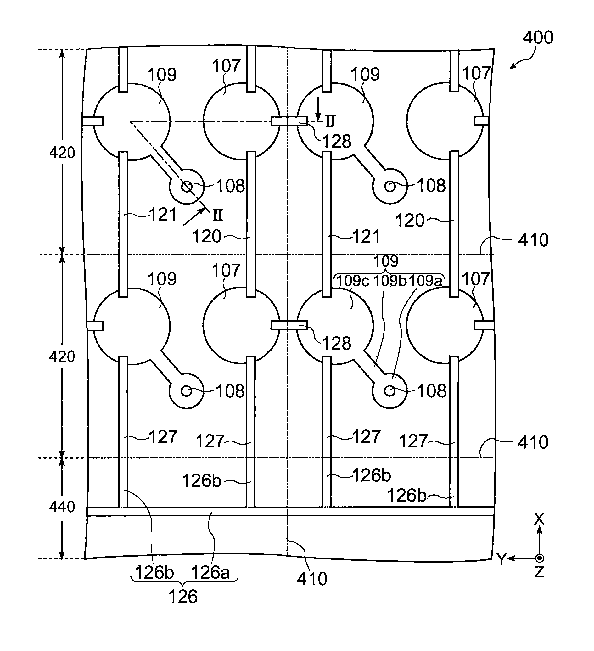
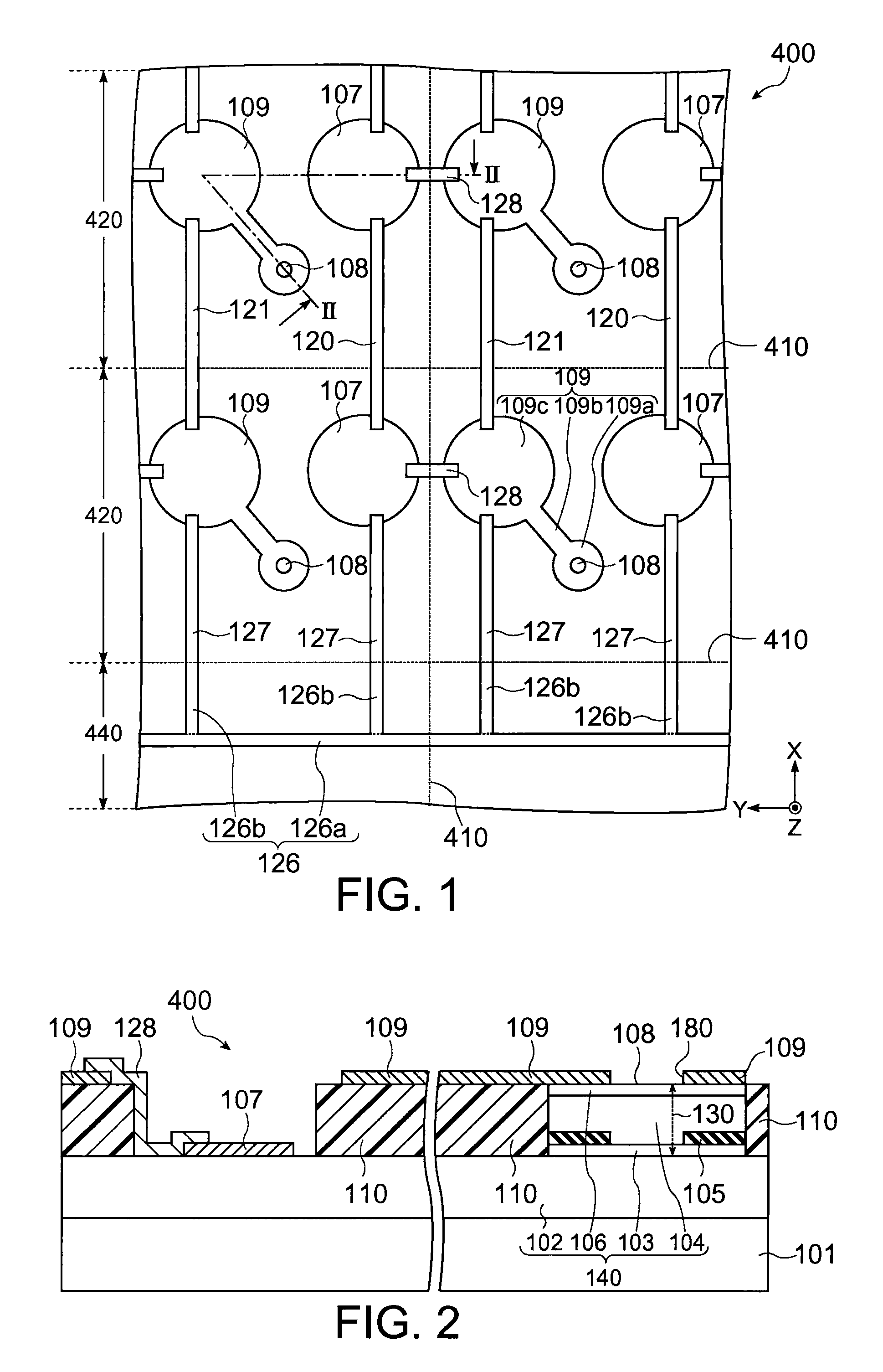
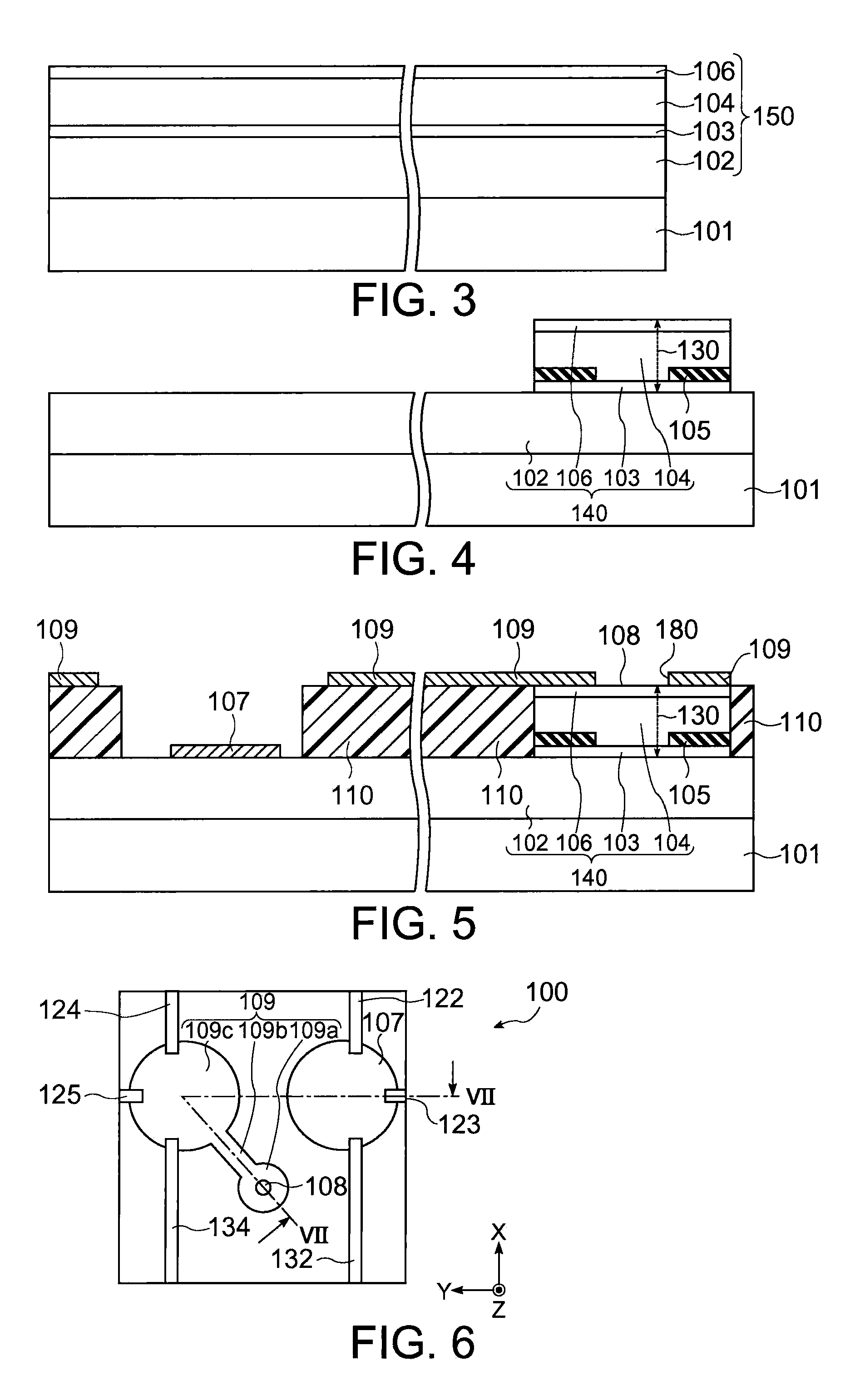
[0031]FIG. 1 schematically shows a plan view of the optical device wafer 400 in accordance with the present embodiment, and FIG. 2 is a cross-sectional view taken along lines II-II of FIG. 1. In the present embodiment, an example in which the optical device wafer 400 is a surface-emitting type semiconductor laser wafer is described.

[0032]The optical device wafer400 may include a plurality of chip regions 420, connecting sections 120, 121 and 128, and a region 440 (non-chip region) other than the chip regions 420. It is noted that FIG. 4 shows four chip regions 420 for the sake of convenience, but the number of the chip regions 420 is not particularly limited.

[0033]Each of the chip regions 420 may include a substrate 101, an optical section (a light emitting section) 140,...


PUM


Abstract

An optical device wafer includes: a plurality of chip regions; and at least one connecting section, wherein the chip region includes a first semiconductor layer of a first conductivity type, an optical layer that emits light or receives light formed above the first semiconductor layer, a second semiconductor layer of a second conductivity type formed above the optical layer, a first electrode electrically connected to the first semiconductor layer, and a second electrode electrically connected to the second semiconductor layer, wherein the connecting section short-circuits the first electrodes, the second electrodes, or the first electrode and the second electrode in adjacent ones of the chip regions.

Description

[0001]The entire disclosure of Japanese Patent Application No. 2006-142303, filed May 23, 2006 is expressly incorporated by reference herein.BACKGROUND[0002]1. Technical Field[0003]The present invention relates to optical device wafers, optical device chips and methods for manufacturing the same.[0004]2. Related Art[0005]An optical device such as a surface-emitting type semiconductor laser itself has a low electrostatic breakdown voltage, such that the device may be damaged by static electricity caused by a machine or an operator in a mounting process. A variety of measures are usually implemented in a mounting process to remove static electricity, but these measures have limitations.[0006]For example, Japanese laid-open patent application JP-A-2004-6548 describes a technology to compose a capacitance device by laminating insulating films and metal films wherein the capacitance device serves as a breakdown voltage device. In this case, it may take a long time for laminating layers t...

Claims


Application Information

Patent Timeline
Patent Type & Authority Patents(United States)
IPC IPC(8): G02B6/12H01L21/00H01L21/82
CPCB82Y20/00H01L31/105H01S5/423H01S5/3432H01S5/4018H01S5/18311H01S5/04256H01S5/02345
Inventor NISHIDA, TETSUO
Owner SEIKO EPSON CORP
Why Eureka
Try Eureka