
Electronic circuit device including electric element and varistor on substrate and its manufacture method

a technology of electrostatic surge and manufacturing method, applied in the direction of resistor details, thin film varistors, emergency protective arrangements for limiting excess voltage/current, etc., can solve the problems of noise, electrostatic surge, and malfunction caused by surge and noise, and electronic components, piezoelectric materials, are likely to generate electrostatic surges

Inactive Publication Date: 2009-08-04
FUJITSU LTD
View PDF14 Cites 6 Cited by
  • Summary
  • Abstract
  • Description
  • Claims
  • Application Information

AI Technical Summary

Benefits of technology

[0014]By forming also a varistor element on the substrate on which an electronic element is formed, even a discrete electronic circuit device can lower instantaneously a surge voltage applied across the pair of electrodes of the electronic element.

Problems solved by technology

Malfunction caused by electrostatic surges and noises is becoming an important issue as a drive frequency of electronic components becomes high.
Electronic components, typically dielectric filters and surface acoustic wave (SAW) filters having piezoelectric material, are likely to generate electrostatic surges because these components have piezoelectric effect that voltage is generated upon application of a stress.
However, a SAW filter itself is not provided with the electrostatic surge countermeasure.
Therefore, the worker feels uncomfortable shocks of electrostatic surges in some cases.

Method used


Image

  • Electronic circuit device including electric element and varistor on substrate and its manufacture method
  • Electronic circuit device including electric element and varistor on substrate and its manufacture method
  • Electronic circuit device including electric element and varistor on substrate and its manufacture method

Examples


first embodiment

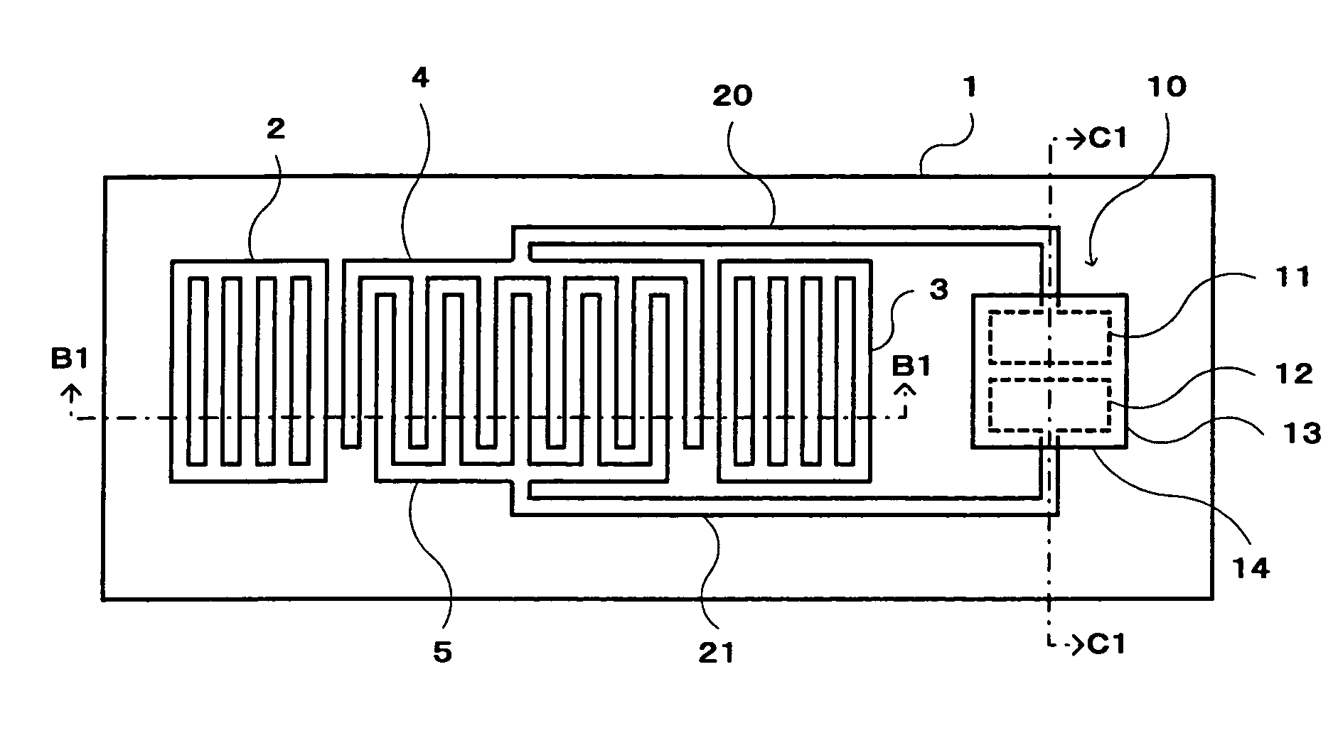
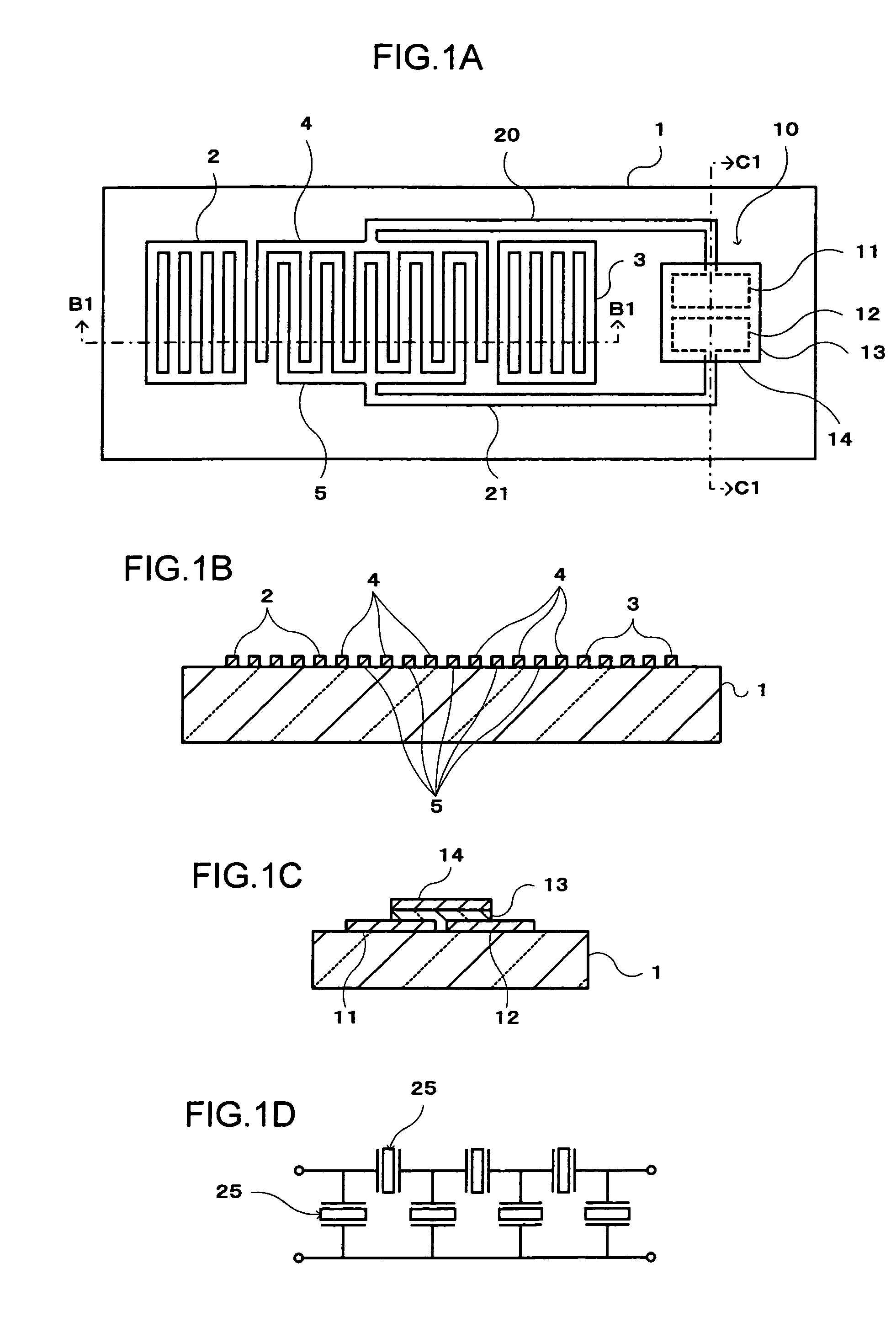
[0022]FIG. 1A is a plan view of an electronic circuit device and FIGS. 1B and 1C are cross sectional views taken along one-dot chain line B1-B1 and one-dot chain line C1-C1 of FIG. 1, respectively. On the surface of a substrate 1 made of lithium tantalate (LiTaO3), a pair of interdigital transducer electrodes 4 and 5 interdigitated with each other is formed. Reflectors 2 and 3 are formed on opposite ends of a path along which a surface acoustic wave excited by the interdigital transducer electrodes 4 and 5 propagates.

[0023]Each of the reflectors 2 and 3 is constituted of a plurality of conductive patterns extending in a direction perpendicular to a propagation direction of the surface acoustic wave. These conductive patterns are electrically shorted. The surface acoustic wave excited by the interdigital transducer electrodes 4 and 5 and propagating toward opposite sides is reflected by the reflectors 2 and 3. Therefore, a standing wave is generated between the paired reflectors 2 a...

second embodiment

[0043]Next, with reference to FIG. 5, description will be made on a manufacture method for an electronic circuit device according to the

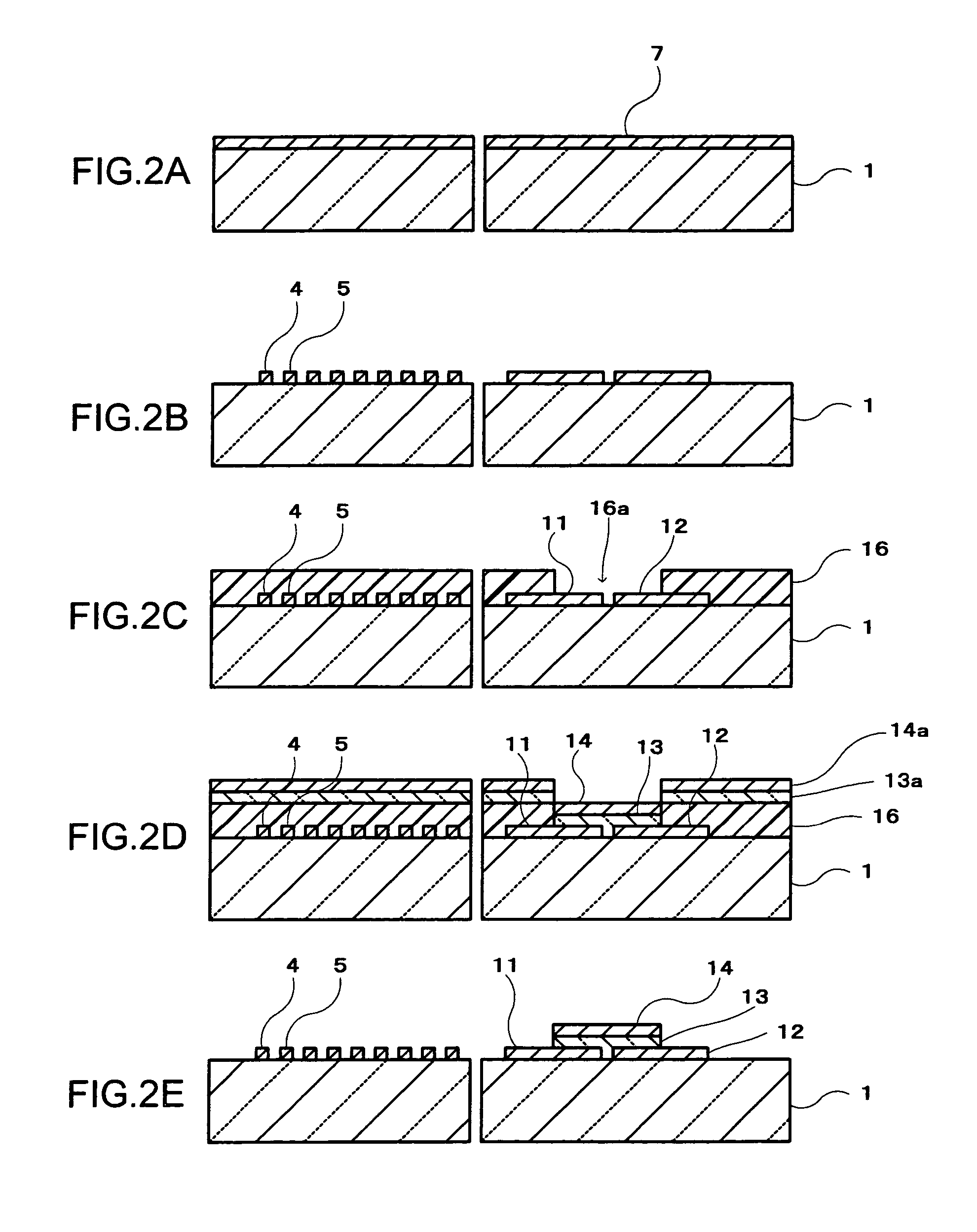
[0044]As shown in FIG. 5A, on the surface of a substrate 60 having an insulating surface, aluminum having a purity of 99.99% is deposited by electron beam evaporation to form an aluminum film having a thickness of 500 nm. This aluminum film is patterned by photolithography to form a lower electrode 63 and pads 61 and 62.

[0045]As shown in FIG. 5B, an aluminum oxide film 65 is formed on the surfaces of the lower electrode 63 and pads 61 and 62. The aluminum oxide film 65 is formed by placing the substrate in the atmospheric air for 24 hours to naturally oxidize the surface of the aluminum. Under this condition, a thickness of the aluminum oxide film 65 is about 3 nm.

[0046]As shown in FIG. 5C, an upper electrode 66 is formed partially covering the lower electrode 63. The upper electrode 66 is formed by depositing aluminum by electron beam evaporation t...

third embodiment

[0053]FIG. 7 is a schematic diagram of an electronic circuit device according to the On the surface of a semiconductor substrate 70, a ferroelectric RAM (FRAM) of one-transistor one-capacitor type is formed. One memory cell of FRAM is constituted of a MOS transistor 71 and a ferroelectric capacitor 72. The source of the MOS transistor 71 is connected to one electrode of the ferroelectric capacitor 72.

[0054]Description will be made on a manufacture method for an electronic circuit device according to the third embodiment. An interlayer insulating film 75 of silicon oxide is formed on a substrate 70, covering a memory cell of FRAM. Via holes are formed in the interlayer insulating film 75 at positions corresponding to the drain and gate of the MOS transistor 71, at a position corresponding to an interconnection point between the source of the MOS transistor 71 and one electrode of the ferroelectric capacitor 72, and at a position corresponding to the other electrode of the ferroelect...


PUM


Abstract

An electronic element having at least a pair of electrodes is formed on a substrate. A varistor element is formed on the substrate, the varistor element including a pair of electrodes and a varistor insulating film. When a surge voltage is applied across the pair of electrodes of the varistor element, a surge current flows through the varistor insulating film. One electrode of the varistor element is connected to one electrode of the electronic element, and the other electrode of the varistor element is connected to the other electrode of the electronic element.

Description

CROSS REFERENCE TO RELATED APPLICATION[0001]This application is based on and claims priority of Japanese Patent Application No. 2005-149729 filed on May 23, 2005, the entire contents of which are incorporated herein by reference.BACKGROUND OF THE INVENTION[0002]A) Field of the Invention[0003]The present invention relates to an electronic circuit device and its manufacture method, and more particularly to an electronic circuit device having a countermeasure against a surge voltage and its manufacture method. The present invention relates also to a manufacture method for a varistor suitable for application to an electronic circuit device and to a manufacture method for a semiconductor device having a varistor.[0004]B) Description of the Related Art[0005]Malfunction caused by electrostatic surges and noises is becoming an important issue as a drive frequency of electronic components becomes high. Electronic components, typically dielectric filters and surface acoustic wave (SAW) filter...

Claims


Application Information

Patent Timeline
Patent Type & Authority Patents(United States)
IPC IPC(8): H01C7/10
CPCH01C1/146H01C7/1013H01C7/102H01C7/115H01C7/12H01L27/0288H01L27/0808H03H3/08H03H9/02921H03H9/0542H01L2224/48091H01L2924/13091H05K1/167H05K1/0254H01L2924/00014H01L2924/00
Inventor KONDO, MASAO
Owner FUJITSU LTD
Learn More