

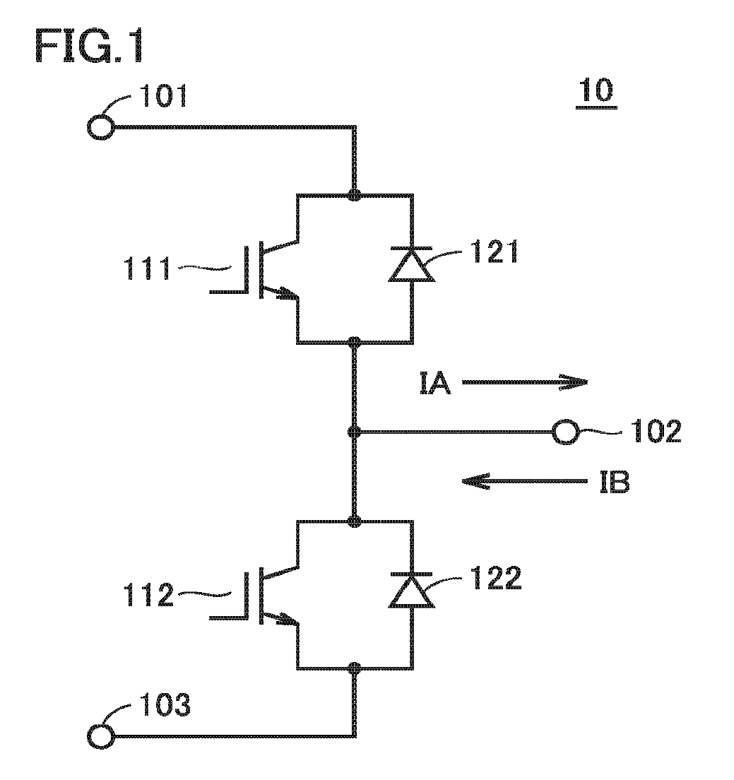
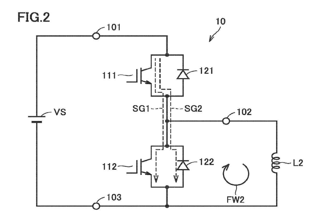
Power semiconductor module
- Summary
- Abstract
- Description
- Claims
- Application Information
AI Technical Summary
Benefits of technology
Problems solved by technology
Method used
Image

Examples
embodiment 1
Modification of Embodiment 1
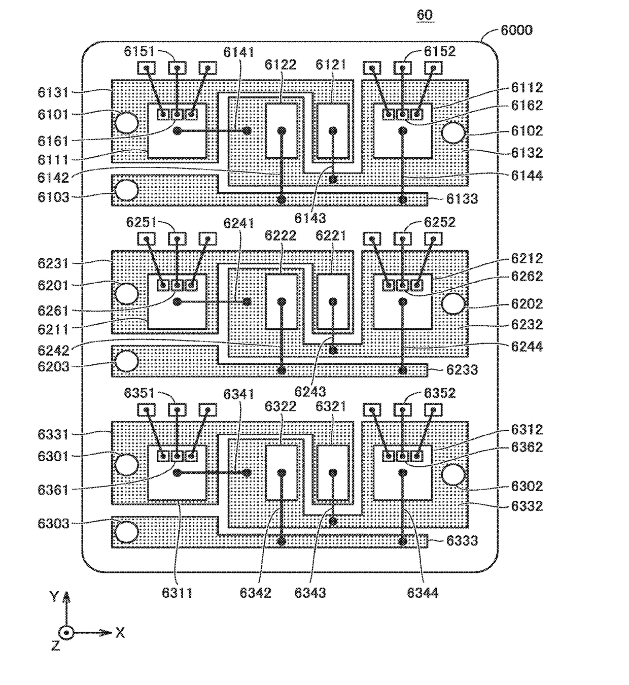
[0066]FIG. 6 is a schematic plan view that shows a layout of Modification of the power semiconductor module of FIG. 4. A power semiconductor module 11 of FIG. 6 is different from the case of FIG. 4 in arrangement of the positive-side diode device 121 and the negative-side diode device 122. Specifically, the case of FIG. 6 is characterized in that the positive-side switching device 111, the negative-side diode device 122, the positive-side diode device 121, and the negative-side switching device 112 are arrayed not substantially in a row, so that the semiconductor devices are disposed closer to each other. Thus, the power semiconductor module can be further downsized.
[0067]Note that the case of FIG. 6 is the same as that of FIG. 4 in that the positive-side diode device 121 and the negative-side diode device 122 are disposed between the positive-side switching device 111 and the negative-side switching device 112. Further, the case of FIG. 6 is also the sam...
embodiment 2
[0069]FIG. 7 is a schematic plan view that shows a layout of a power semiconductor module according to Embodiment 2.
[0070]A power semiconductor module 20 of FIG. 7 is a modification of the power semiconductor module 10 of FIG. 4. Specifically, an insulating substrate 200, a positive-side power-supply terminal 201, an output terminal 202, and a negative-side power-supply terminal 203 of FIG. 7 respectively correspond to the insulating substrate 100, the positive-side power-supply terminal 101, the output terminal 102, and the negative-side power-supply terminal 103 of FIG. 4. A positive-side switching device 211, a negative-side switching device 212, a positive-side diode device 221, and a negative-side diode device 222 of FIG. 7 respectively correspond to the positive-side switching device 111, the negative-side switching device 112, the positive-side diode device 121, and the negative-side diode device 122 of FIG. 4. A positive-side conductive pattern 231, an output-side conductive...
embodiment 3
Modification of Embodiment 3
[0097]FIG. 12 is a schematic plan view that shows a layout of Modification of the power semiconductor module of FIG. 11. A power semiconductor module 31 of FIG. 12 is characterized in that the positive-side switching device 311, the negative-side diode device 322, the positive-side diode device 321, and the negative-side switching device 312 are arrayed not substantially in a row, so that the semiconductor devices are disposed closer to each other. Thus, the power semiconductor module can be further downsized.
[0098]Note that the case of FIG. 12 is the same as that of FIG. 11 in that the positive-side diode device 321 and the negative-side diode device 322 are disposed between the positive-side switching device 311 and the negative-side switching device 312. Further, the case of FIG. 12 is also the same as that of FIG. 11 in that the negative-side diode device 322 is disposed closer to the positive-side switching device 311 than the positive-side diode dev...
PUM
 Abstract
Description
Claims
Application Information