RCD buffering circuit of Z-source inverter and Z-source inverter topology circuit comprising buffering circuit

A source inverter and snubber circuit technology, applied in the field of snubber circuits, can solve the problems of DC link voltage slopes, large losses, and high DC link voltage values, and achieve the goals of avoiding voltage distortion, reducing surge voltage, and low loss Effect

Active Publication Date: 2014-10-08
HARBIN INST OF TECH
View PDF5 Cites 7 Cited by
  • Summary
  • Abstract
  • Description
  • Claims
  • Application Information

AI Technical Summary

Problems solved by technology

[0003] The present invention is to solve the problem that RC, RCD and RCD limiter type buffer circuits will have a slope in the DC link voltage when the Z source inverter is used, the DC link voltage value is too high and the loss is large, and the Z source inverter RCD is now provided. Snubber circuit and Z-source inverter topology circuit containing the snubber circuit

Method used


Image

  • RCD buffering circuit of Z-source inverter and Z-source inverter topology circuit comprising buffering circuit
  • RCD buffering circuit of Z-source inverter and Z-source inverter topology circuit comprising buffering circuit

Examples


specific Embodiment approach 1

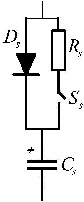
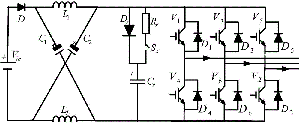
[0023] Specific implementation mode one: refer to figure 1 Specifically illustrate this embodiment, the Z source inverter RCD snubber circuit described in this embodiment, it comprises: Diode D S , resistance R S and capacitance C S ;

[0024] The diode D S The positive connection resistor R S One end of the diode D S The negative terminal of the connected capacitor C S one end of

[0025] It also includes: Switch S S ;

[0026] Resistance R S The other end of the switch S is connected S One end of the switch S S The other end of the diode D is connected simultaneously S The negative pole and the capacitor C S one end of

[0027] Diode D S The positive terminal and the resistor R S One end of the Z source inverter RCD snubber circuit at the same time as the positive;

[0028] Capacitance C S The other end of the Z source inverter is used as the negative electrode of the RCD snubber circuit.

specific Embodiment approach 2

[0029] Specific embodiment two: this embodiment is to further explain the Z source inverter RCD snubber circuit described in specific embodiment one, in this embodiment, the switch S S for IGBTs.

[0030] IGBT (Insulated Gate Bipolar Transistor), an insulated gate bipolar transistor, has the advantages of high input impedance of MOSFET and low conduction voltage drop of GTR, with low driving power and low saturation voltage.

specific Embodiment approach 3

[0031] Specific embodiment three: this embodiment is to further explain the Z source inverter RCD snubber circuit described in specific embodiment one, in this embodiment, the switch S S for MOSFETs.

[0032] MOSFET (Metal-Oxide-Semiconductor Field-Effect Transistor, MOSFET), Metal-Oxide-Semiconductor Field-Effect Transistor, the driving power is small, and the switching speed is fast.


PUM


Abstract

The invention provides an RCD buffering circuit of a Z-source inverter and a Z-source inverter topology circuit comprising the buffering circuit, and relates to the buffering circuit of the Z-source inverter. The buffering circuit aims to solve the problems that direct-current link voltage of RC, RCD and RCD amplitude limiting type buffering circuits for the Z-source inverter generates a slope, the value of the direct-current link voltage is excessively high, and the loss is large. According to the RCD buffering circuit of the Z-source inverter and the Z-source inverter topology circuit comprising the buffering circuit, a non-inductive resistor and a switch device in a traditional RCD buffering circuit are connected in series and then connected with a fast recovery diode in parallel, and then the whole is connected with a non-inductive capacitor in series and then connected to a direct-current bus side of the Z-source inverter in parallel. The switch device additionally arranged is connected when the Z-source inverter is in a non-direct connection state, and disconnected when the Z-source inverter is in a direct connection state. The problems of the voltage distortion, the excessively high voltage value and the large direct connection loss generated when the traditional buffering circuit is applied to the Z-source inverter can be solved. The buffering circuit is suitable for the Z-source inverter medium and small in power.

Description

technical field [0001] The invention relates to a buffer circuit of a Z source inverter. Background technique [0002] When the traditional C-type snubber circuit is applied to the Z-source inverter, when the through state comes, it is equivalent to directly short-circuiting the charged capacitor, and the current impact on the switch tube and capacitor is very large. When the DC link voltage level is high, the switch tube may even be burned. Moreover, in the application occasions of medium and high power level converters, the C-type snubber circuit is easy to form an oscillation with the stray inductance of the main circuit. RC, RCD and RCD limiter snubber circuits will have the problems of DC link voltage slope, high DC link voltage value and large loss when Z source inverter is used. Contents of the invention [0003] The present invention is to solve the problem that RC, RCD and RCD limiter type buffer circuits will have a slope in the DC link voltage when the Z sourc...

Claims


Application Information

Patent Timeline
Patent Type & Authority Applications(China)
IPC IPC(8): H02M1/34H02M7/5387
Inventor 张千帆董帅周超伟那拓扑李为汉
Owner HARBIN INST OF TECH
Why Eureka
Try Eureka