Switching device

a technology of switching device and recovery current, which is applied in the direction of power conversion systems, electrical devices, and arrangements responsive to excess voltage, can solve the problems of limiting the power dissipation associated with recovery current, and achieve the effects of reducing surge voltage, simple configuration, and reducing power dissipation

Active Publication Date: 2013-09-24
DENSO CORP
View PDF15 Cites 9 Cited by
  • Summary
  • Abstract
  • Description
  • Claims
  • Application Information

AI Technical Summary

Benefits of technology

[0009]In view of the foregoing problems, it is an object of the present invention to provide a switching device that can reduce power dissipation associated with a recovery current while reducing a surge voltage, with a simple configuration.

Problems solved by technology

In addition, power dissipation associated with a recovery current can be restricted by coupling the snubber circuit in the above-described manner.

Method used


Image

  • Switching device
  • Switching device
  • Switching device

Examples


first embodiment

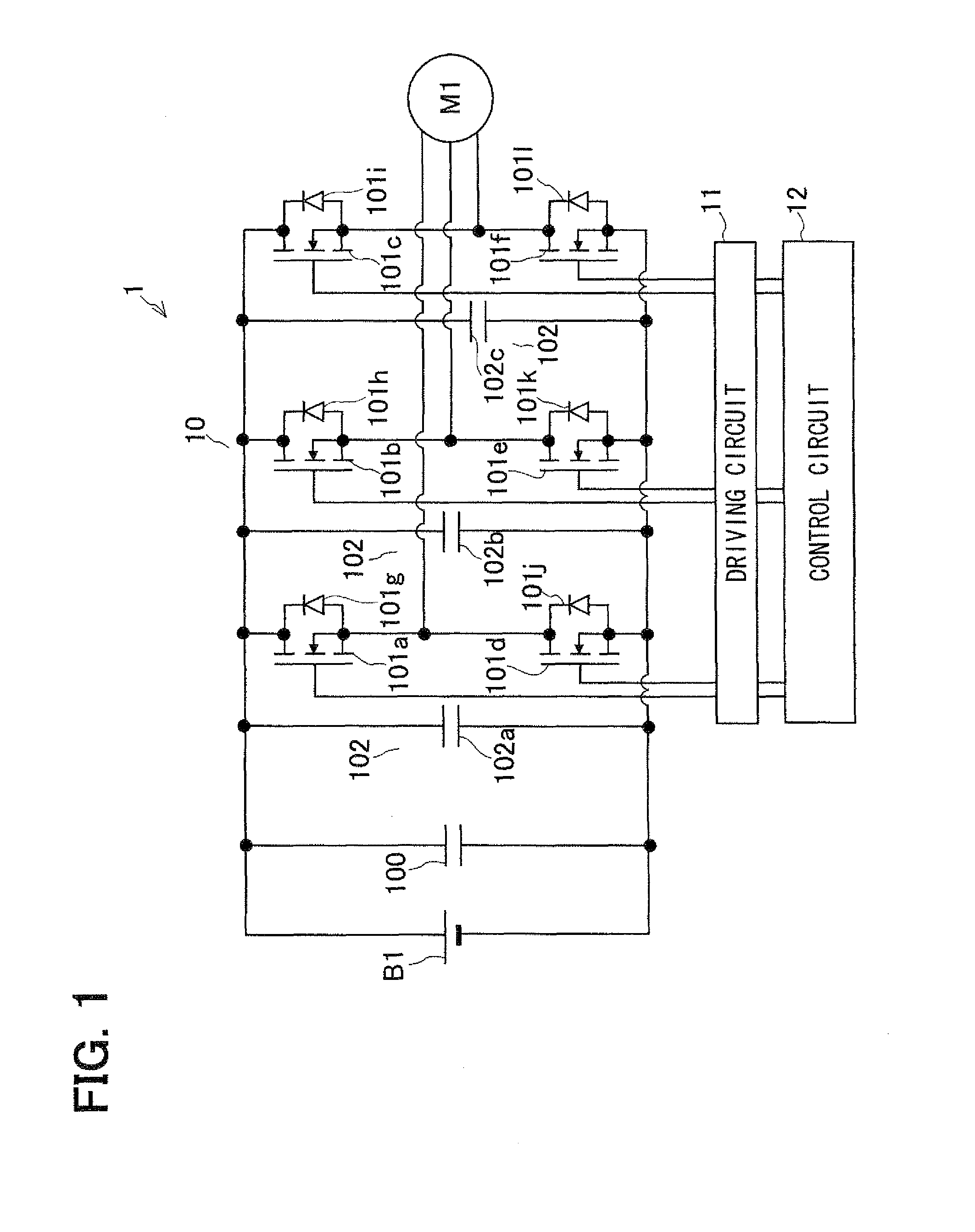
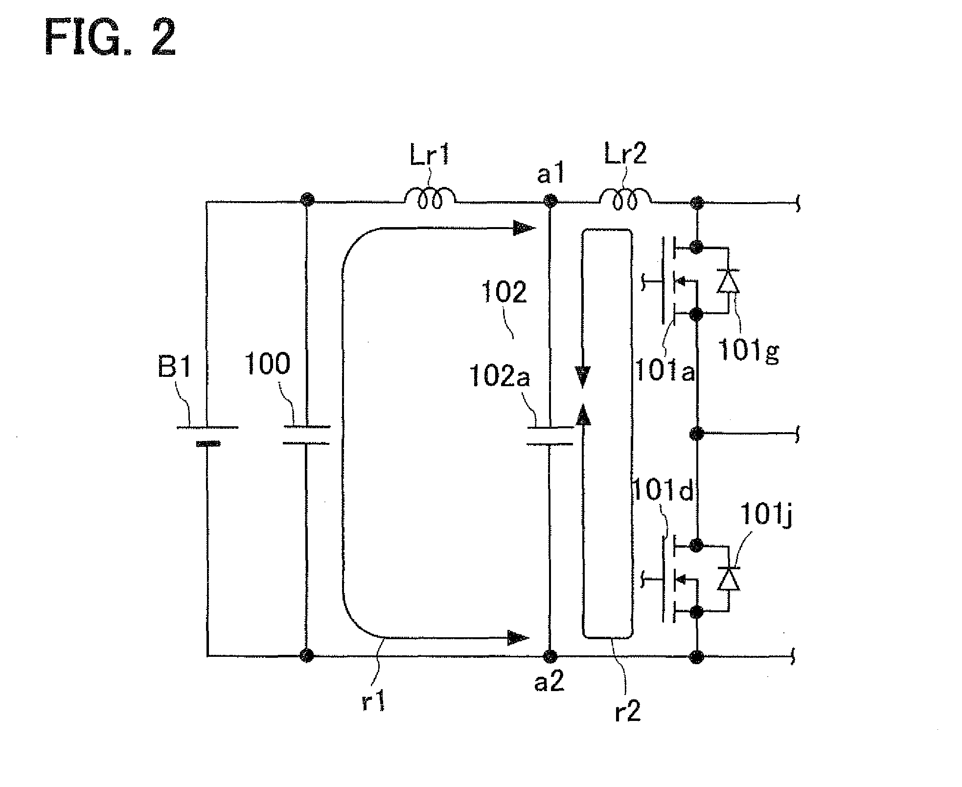
[0031]A switching device according to a first embodiment of the present invention can be suitably used for, for example, a motor control device disposed in a vehicle. A motor control device 1 according to the present embodiment will be described with reference to FIG. 1 and FIG. 2.

[0032]A three-phase alternating current (AC) motor M1 shown in FIG. 1 is disposed in a vehicle. The three-phase AC motor M1 generates driving force when three-phase AC voltage is supplied.

[0033]The motor control device 1 is disposed in a vehicle. The motor control device 1 can operate as a power converter. The motor control device 1 converts direct current (DC) voltage output from a battery 61 (direct current power source) into three-phase AC voltage and supplies the three-phase AC voltage to three-phase AC motor M1. In other words, the motor control device 1 converts DC power to AC power and supplies the AC power to the three-phase AC motor M1. The motor control device 1 includes an inverter circuit 10, a...

second embodiment

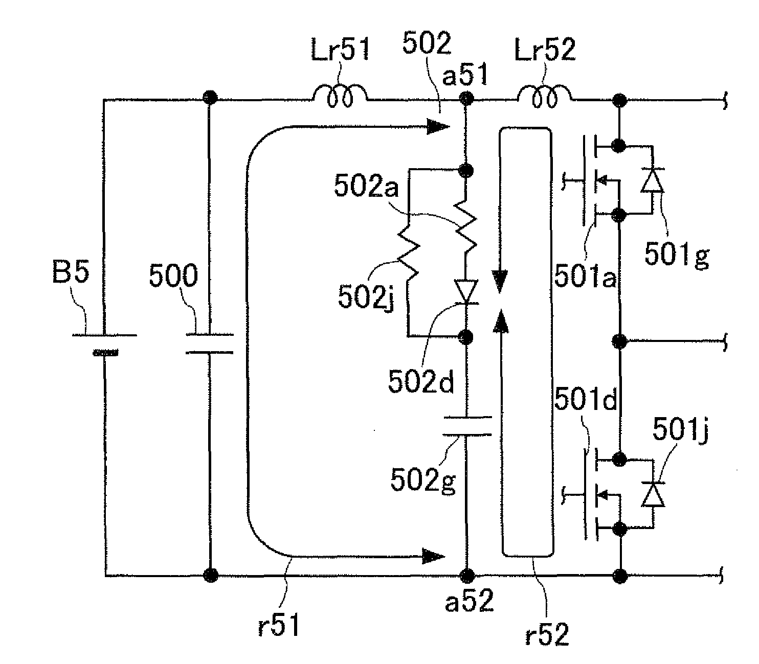
[0054]A motor control device 2 according to a second embodiment of the present invention will be described with reference to FIG. 6 and FIG. 7. In the motor control device 2, a configuration of a snubber circuit is different from the configuration of the snubber circuit 102 according to the first embodiment.

[0055]As shown in FIG. 6, the motor control device 2 includes an inverter circuit 20, a driving circuit 21, and a control circuit 22. The inverter circuit 20 can operate as a switching device. The driving circuit 21 and the control circuit 22 have configurations similar to the configurations of the driving circuit 11 and the control circuit 12 according to the first embodiment. The inverter circuit 20 is coupled with a battery B2 and a three-phase AC motor M2.

[0056]The inverter circuit 20 includes a smoothing capacitor 200, FETs 201a-201f, and a snubber circuit 202. The FETs 201a-201f can operate as semiconductor switching elements. The smoothing capacitor 200 has a configuration...

third embodiment

[0063]A motor control device 3 according to a third embodiment of the present invention will be described with reference to FIG. 9 and FIG. 10. In the motor control device 3, a configuration of a snubber circuit is different from the configuration of the snubber circuit 102 according to the first embodiment.

[0064]As shown in FIG. 9, the motor control device 3 includes an inverter circuit 30, a driving circuit 31, and a control circuit 32. The inverter circuit 30 can operate as a switching device. The driving circuit 31 and the control circuit 32 have configurations similar to the configurations of the driving circuit 11 and the control circuit 12 according to the first embodiment. The inverter circuit 30 is coupled with a battery B3 and a three-phase AC motor M3.

[0065]The inverter circuit 30 includes a smoothing capacitor 300, FETs 301a-301f, and a snubber circuit 302. The FETs 301a-301f can operate as semiconductor switching elements. The smoothing capacitor 300 has a configuration...


PUM


Abstract

A switching device includes a plurality of semiconductor switching elements coupled in series, a smoothing capacitor, and snubber circuit. Each of the semiconductor switching elements includes a free wheel diode. The smoothing capacitor is coupled in parallel with a direct current power source and the semiconductor switching elements. The smoothing capacitor smoothes an output of the direct current power source and supplies the smoothed output to the semiconductor switching elements. The snubber circuit is coupled between a first connecting point and a second connecting point in parallel with the semiconductor switching elements. An inductance of a first channel provided from the first connecting point to the second connecting point through the smoothing capacitor is equal to or more than 10 times as large as an inductance of a second channel including the semiconductor switching elements and the snubber circuit.

Description

CROSS REFERENCE TO RELATED APPLICATIONS[0001]The present application is based on and claims priority to Japanese Patent Applications No. 2010-14568 filed on Jan. 26, 2010 and No. 2010-261114 filed on Nov. 24, 2010, the contents of which are incorporated in their entirety herein by reference.BACKGROUND OF THE INVENTION[0002]1. Field of the Invention[0003]The present invention relates to a switching device including a plurality of semiconductor switching elements coupled in series.[0004]2. Description of the Related Art[0005]Japanese Patent No. 2,754,411 (corresponding to U.S. Pat. No. 5,077,651) discloses a power converter as a switching device that includes a plurality of semiconductor elements coupled in series. As shown in FIG. 17, the power converter includes two transistors Tr1 and Tr2 coupled in series. A collector of the transistor Tr1 is coupled with a positive terminal of a direct current power source VDC. An emitter of the transistor Tr2 is coupled with a negative terminal ...

Claims


Application Information

Patent Timeline
Patent Type & Authority Patents(United States)
IPC IPC(8): H02H7/00
CPCH02M7/003H02M7/5387
Inventor YAMAGUCHI, NOBUHISA
Owner DENSO CORP
Why Eureka
Try Eureka