Optical modulation element module

a technology module, which is applied in the field of optical modulation element module, can solve the problems of light dispersion in a fiber, higher driving voltage, and low modulation efficiency, and achieve the effects of reducing the line impedance of the modulation electrode, widening the frequency response properties, and facilitating the acquisition of broader band components

Inactive Publication Date: 2009-08-04
SUMITOMO OSAKA CEMENT CO LTD
View PDF8 Cites 1 Cited by
  • Summary
  • Abstract
  • Description
  • Claims
  • Application Information

AI Technical Summary

Benefits of technology

[0030]According to the first aspect of the invention, the modulation signal input unit corresponding to the two electrodes is formed as one terminal, and the modulation signal from the modulation signal input unit is divided into two signals and applied to each modulation electrode by the transformer branching unit. Accordingly, only one terminal for inputting the modulation signal is needed as the optical modulator having a single modulation electrode and the optical modulation element may be simply treated. Furthermore, because the optical modulation element is driven by two modulation electrodes, the driving voltage can be reduced and the modulation efficiency can be improved.
[0032]According to the third aspect of the invention, in a region which one of the branched waveguide of the MZ type optical modulation element is formed, the crystal axis of the substrate is domain-inverted. In the transformer branching unit, the electric power branching ratio of the output port is 1:1 and the phase difference of each branched signal is 0° (hereinafter, referred to as synchronous type transformer branching unit). Accordingly, it is possible to realize the optical modulator with low chirp and a low driving voltage, which is similar to the second aspect, and for the synchronous type transformer branching unit, it may be easier to obtain broader band components and it may be possible to realize wider frequency response properties of the optical modulator than the reverse-phase type transformer branching unit.
[0033]According to the fourth aspect of the invention, in the transformer branching unit, the input impedance is matched with the impedance of the modulation signal input unit and the output impedance is matched with the line impedance of each modulation electrode with the impedance value of 50 Ω or less. Accordingly, it is possible to control the reflection of the modulation signal in the connection of the line, and to supply an optical modulator having a high frequency property by matching the respective impedances. Furthermore, it is possible to use design of a dual modulator of related art by reducing the line impedance of the modulation electrode of the optical modulation element, to 50 Ω or less. Furthermore, it is possible to reduce the interval between the modulation electrode and the ground electrode of the optical modulation element by reducing the line impedance of the modulation electrode. It is also possible to realize high-efficiency modulation by increasing the distribution of the electric field which is applied to the waveguide. As the result, it is possible to further reduce the corresponding line impedance to a lower value, and it is possible to further reduce the driving voltage of the optical modulation element by matching the impedances between the transformer branching unit and the modulation electrode.
[0034]According to fifth aspect of the invention, because the substrate of the MZ type optical modulation element is a Z-cut LiNbO3 substrate, it is possible to provide an optical modulator having higher modulation efficiency and more stabilized operation properties than the case of using an X-cut substrate or a substrate other than the LiNbO3 substrate.
[0035]According to the sixth aspect of the invention, because the transformer branching unit uses the transmission line type transformer, a high frequency signal may be branched in the broadband with low loss. For example, it is possible to provide the optical modulator having several tens of MHz to 1 GHz operating bandwidth required when transmitting optical CATV.

Problems solved by technology

In an analog optical transmission system, when an optical CATV transmission system is placed in 1.55 μm band, a problem occurs in the light dispersion in a fiber.
The X-cut LN modulator shown in FIG. 1 generally has low modulation efficiency, thus, it has a problem in that the driving voltage becomes higher.
When integrating phase modulators, it is difficult to reduce the driving voltage due to the structure of the X-cut LN modulator.
There is a problem in that the phase modulation unit occupies most of the interaction length and the interaction length of the intensity modulation unit is restricted.
However, it is difficult to obtain the two-output type driver, which may have higher properties over the large bandwidth and low price, and the two-output type driver is much more expensive than a single output type driver.
Generally, there are problems in that elements such as a phase shifter and the like are needed to obtain optimal modulation, and configuration or adjustment of the circuit becomes complicated.
For example, when the input impedance is 50 Ω, each line impedance is 100 Ω. Especially, in coplanar waveguide (CPW) which is widely used in an LN modulator, there are problems, in that it is difficult to simultaneously satisfy conditions such as high impedance, speed matching of the electric signal with the light wave, and high modulation efficiency, and so on due to the dielectric constant of the LN substrate.

Method used


Image

  • Optical modulation element module
  • Optical modulation element module
  • Optical modulation element module

Examples


Embodiment Construction

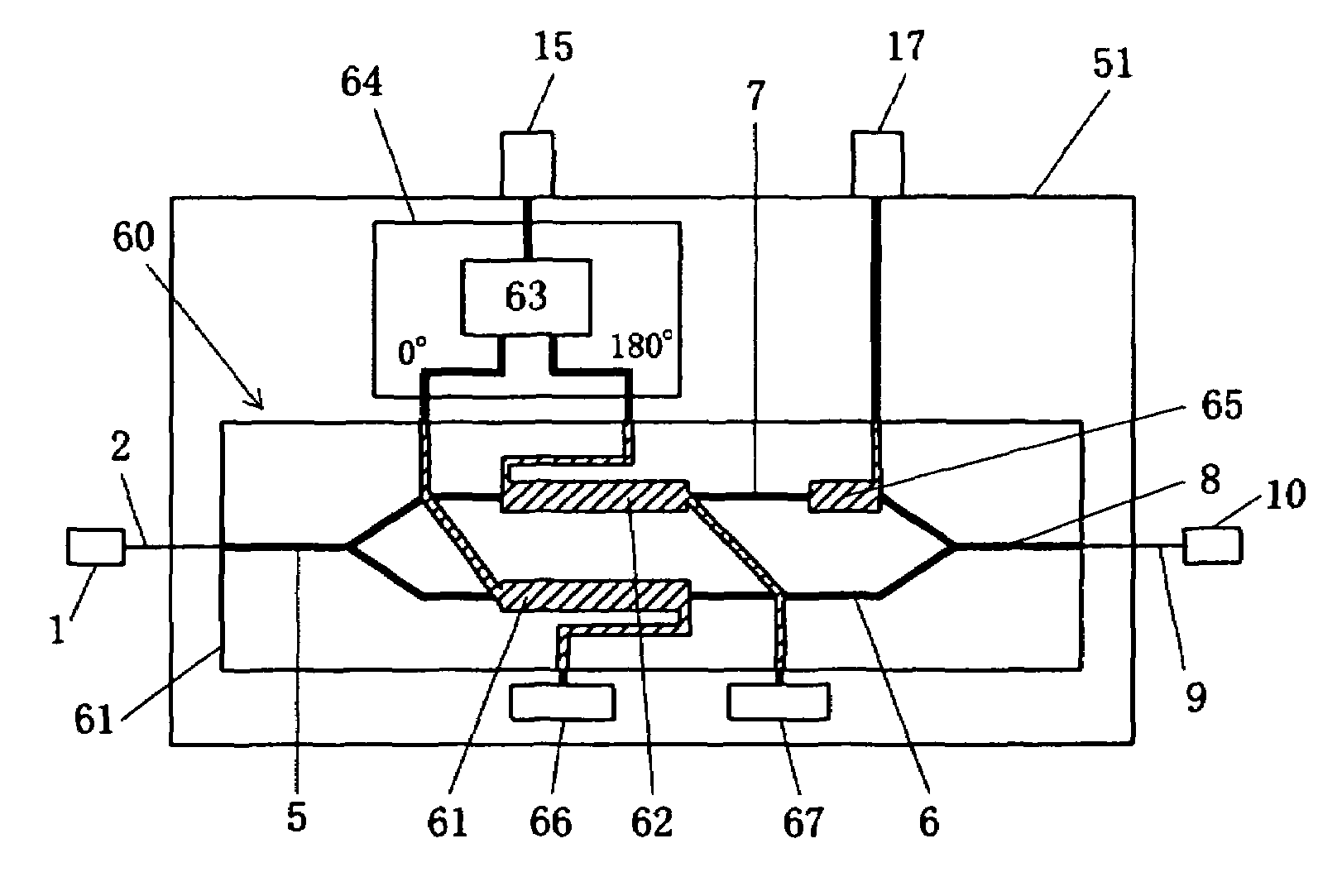
[0061]Hereinafter, an optical modulation element module according to an embodiment of the invention will be described in detail.

[0062]FIG. 4 is a block diagram schematically showing an optical modulation element module according to the embodiment of the invention.

[0063]As shown in FIG. 4, a modulation signal input unit 56 for inputting a modulation signal, a transformer branching unit 57 for dividing the modulation signal into two signals, an MZ type optical modulation element 50 which uses electro-optical effect, and optical input and output units such as optical fibers, and so on are integrated to be placed in a metal case 51 as a single package.

[0064]The modulation signal inputted in the modulation signal input unit 56 is divided into two signals by the transformer branching unit 57 in a modulator which is a transformer type branching element to feed powers to the modulation electrodes of the optical modulation element 50. On the other hand, a light component outputted from an op...


PUM

PropertyMeasurementUnit
impedanceaaaaaaaaaa
line impedanceaaaaaaaaaa
output impedanceaaaaaaaaaa

Abstract

The present invention provides an optical modulation element module which is capable of the optical modulation for analog transmission with a low driving voltage and low chirp.An optical modulation element module, in which Mach-Zehnder type optical modulation element 50 having a Mach-Zehnder type waveguide unit having two branched waveguides on a substrate which has electro-optical effect and two modulation electrodes which apply a modulation signal to each branched waveguide, optical input and output units for inputting and outputting a light wave to and from the optical modulation element, and a modulation signal input unit 56 for inputting the modulation signal into the modulation electrodes are placed in a case 51, includes a transformer branching unit 57 in which the modulation signal input unit which corresponds to the two modulation electrodes is formed as one terminal and which divides the modulation signal from the modulation signal input unit into two signals, and applies the divided modulation signals to each modulation electrode.

Description

BACKGROUND OF THE INVENTION[0001]1. Field of the Invention[0002]The present invention relates to an optical modulation element module, more particularly, to an optical modulation element module capable of being suitably used in an analog optical transmission system.[0003]2. Description of the Related Art[0004]In an analog optical transmission system, when an optical CATV transmission system is placed in 1.55 μm band, a problem occurs in the light dispersion in a fiber. Therefore, a modulation method which uses an external modulator for acquiring preferable transmission properties has been used. In modulators used for the above method, it is important to prevent wavelength chirping which is generated by intensity modulation. For this reason, Mach-Zehnder type external optical modulator (hereinafter, referred to as MZ type optical modulation element) using LiNbO3 (hereinafter, referred to as LN), in which the wavelength chirping is hardly generated, is widely used.[0005]The MZ optical...

Claims


Application Information

Patent Timeline
Patent Type & Authority Patents(United States)
IPC IPC(8): G02F1/035
CPCG02F1/2255G02F2202/20G02F2201/126G02F2001/212G02F1/212
Inventor MIYAZAKI, NORIKAZUYOKOZAWA, MASATAKA
Owner SUMITOMO OSAKA CEMENT CO LTD
Why Eureka
Try Eureka