

Microwave plasma processing device and plasma processing gas supply member
a technology of plasma processing and plasma, which is applied in the field of microwave plasma processing devices, can solve the problems of complicated operation, difficult control of processing conditions, and complicated device configuration, and achieve good energy efficiency
- Summary
- Abstract
- Description
- Claims
- Application Information
AI Technical Summary
Benefits of technology
Problems solved by technology
Method used
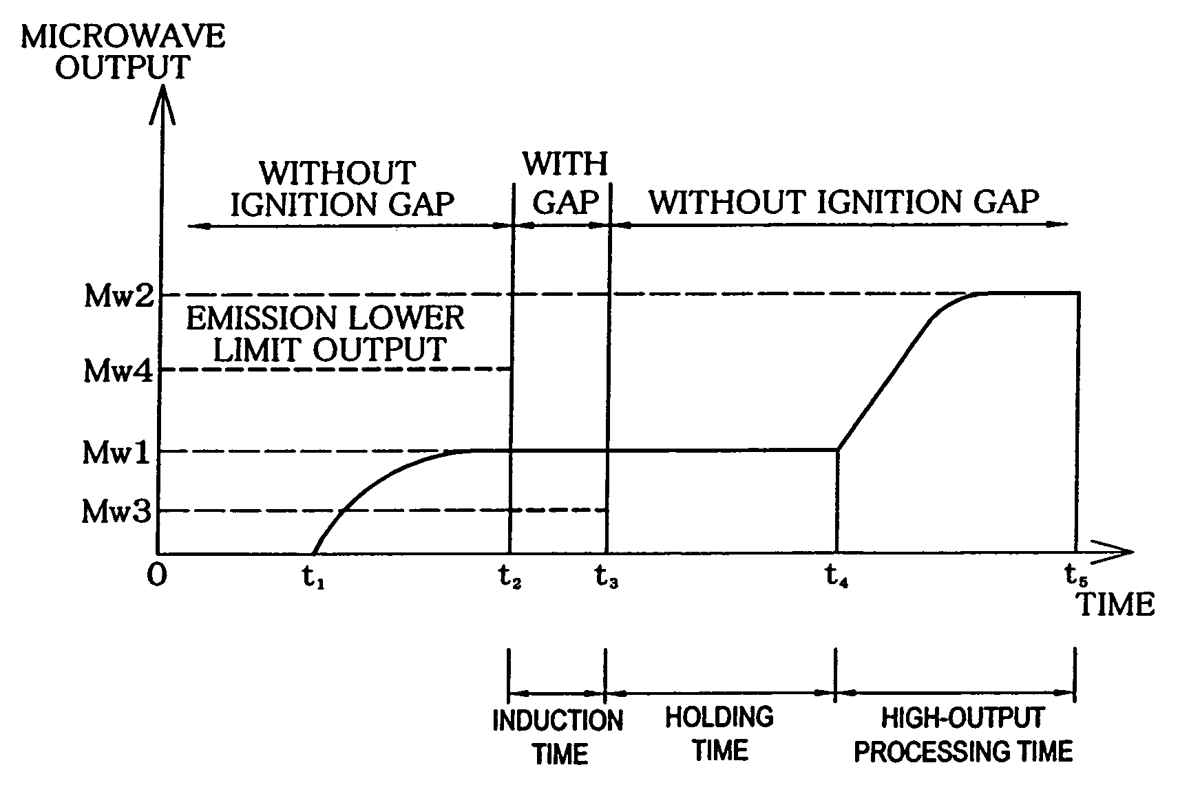
Image

Examples
first embodiment
[0070]First, a microwave plasma processing device according to a first embodiment of the present invention will be described with reference to FIGS. 1 and 2.
[0071]This embodiment is an embodiment in which the microwave plasma processing device according to the present invention is applied to bottle inner surface processing. As a bottle in this embodiment, there is a biaxial-drawing-blow-molded bottle formed of polyester such as polyethylene terephthalate.
[Microwave Plasma Processing Device]
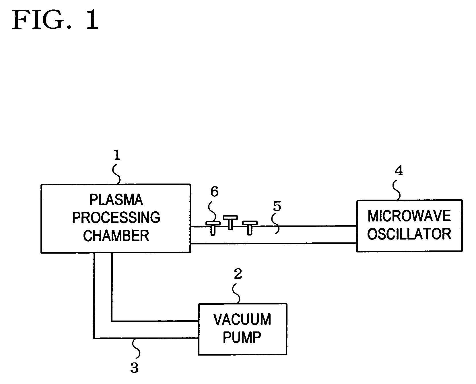
[0072]FIG. 1 is a schematic arrangement plan of the microwave plasma processing device according to this embodiment.
[0073]A vacuum pump 2 which performs emission of a gas in a processing chamber 1 and maintains the inside of this chamber in a depressurized state is connected with the plasma processing chamber 1 through an exhaust pipe 3. Further, a microwave oscillator 4 is connected through a waveguide tube 5 which is microwave introducing means.
[0074]The microwave oscillator 4 is not restricted ...
experimental example 1
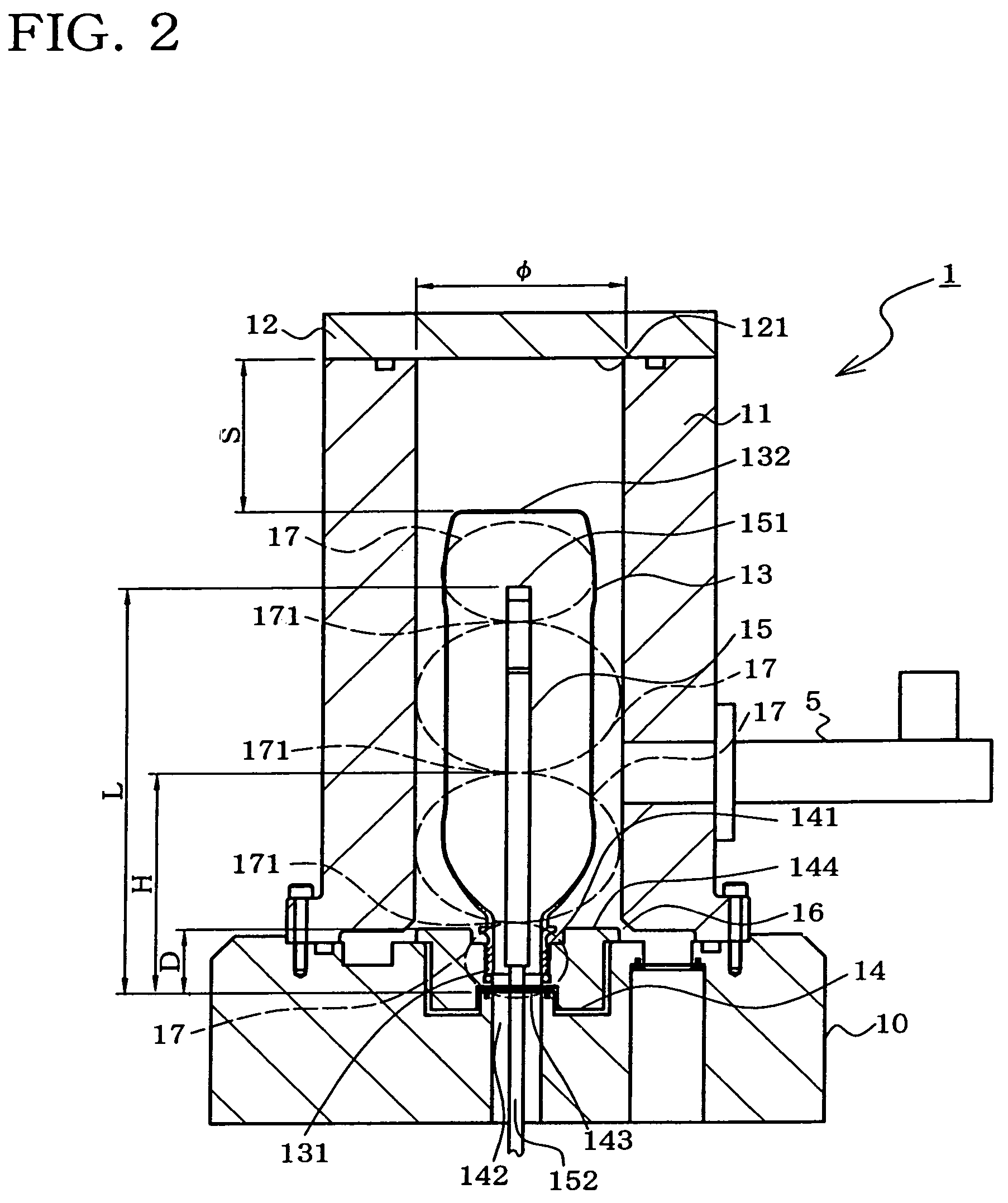
[0146]In the microwave plasma processing device shown in FIG. 2, the plasma processing was conducted with respect to PET bottles having inner capacities of 500 ml (Experiments 1-1 to 1-3) and 350 ml (Experiment 1-4) by using a chamber 11 having a dimension with which a distance (S) between a bottom portion 132 of the bottle having an internal diameter of φ90 mm and an inner capacity of 500 ml and a hood lower surface 121 is 75 mm, bottle fixing means 14 and a processing gas supply member 15 with which a distance (D) from an upper surface 144 of the bottle fixing means 14 to a microwave sealing member 143 and a distance (L) from the microwave sealing member 143 to a gas supply member end portion 151 become values shown in Table 1.
[0147]As an evaluation, whether plasma emission is possible and a reflection intensity of the microwave which can be considered to be returned without being used for the plasma processing were checked.
[0148]Furthermore, in regard to conditions under which th...
experimental example 2
[0157]A bottle was set in the same device as that of Experimental Example 1, the dimension (D) was set to values shown in Table 2, and the dimension (L) with which the reflection intensity of the microwave becomes minimum with respect to each dimension (D) was checked by using a PET bottle having a capacity of 500 ml.
[0158]Furthermore, excellent combinations of the dimensions (D) and (L) were obtained by using commercially available spread sheet software based on this result.
[0159]Table 2 shows a result.
[0160]
TABLE 2D20253035404550(mm)L192185180179180182186(mm)
PUM
| Property | Measurement | Unit |
|---|---|---|
| distance | aaaaa | aaaaa |
| distance | aaaaa | aaaaa |
| distance | aaaaa | aaaaa |
Abstract
Description
Claims
Application Information