Magnetic memory device and method of fabricating the same

a magnetic memory and memory device technology, applied in the field of magnetic memory devices, can solve the problems of deviations occurring among unit cells arranged in second-dimensional patterns, difficulty in achieving alignment, and difficulty in achieving efficient arrangement of mtj structur

Inactive Publication Date: 2009-09-01
SAMSUNG ELECTRONICS CO LTD
View PDF7 Cites 16 Cited by
  • Summary
  • Abstract
  • Description
  • Claims
  • Application Information

AI Technical Summary

Problems solved by technology

However, it may be difficult to accomplish an efficient arrangement among the MTJ structure 10 and the digit and bit lines 3 and 13.
Nevertheless, with the above conventional approach, there still may be difficulties in achieving an alignment among the MTJ structure 10 and the lines 3 and 13 because of a coupling effect which may occur between the MTJ structure 10 and the digit line 3 and between the bit line 13 and the MTJ structure 10.
The above-mentioned alignment difficulty may result in deviations occurring among the unit cells arranged in second-dimensional patterns.
Such alignment deviations may increase as the magnetic memory device become more highly integrated, which in turn may cause program disturbance such as the program failure of selected cells or data changes of deselected cells.
Consequently, the above program disturbance may result in an increase in the defect rate of the magnetic memory device.

Method used


Image

  • Magnetic memory device and method of fabricating the same
  • Magnetic memory device and method of fabricating the same
  • Magnetic memory device and method of fabricating the same

Examples


Embodiment Construction

[0029]Exemplary embodiments of the present invention will be described below in more detail with reference to the accompanying drawings. The present invention may, however, be embodied in different forms and should not be constructed as limited to the exemplary embodiments set forth herein.

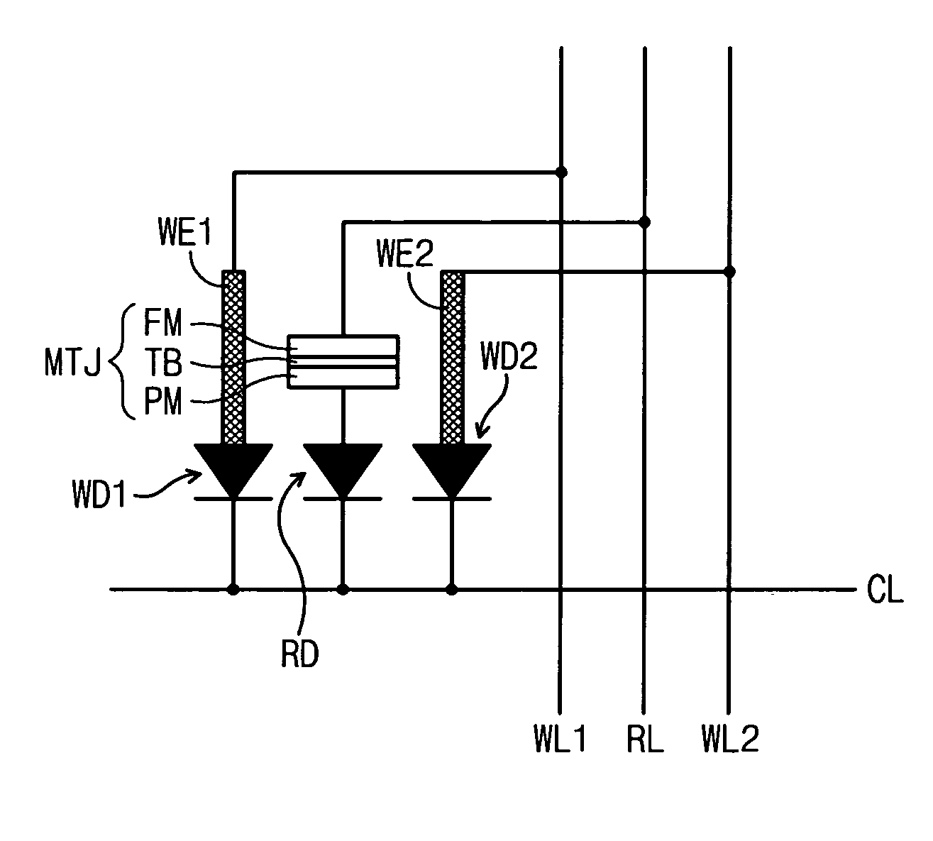
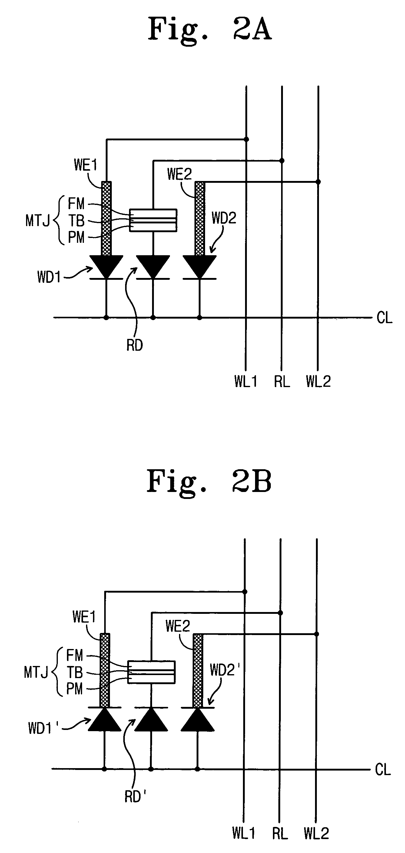
[0030]FIG. 2A is an electrically equivalent circuit illustrating a unit cell in accordance with an exemplary embodiment of the invention, and FIG. 3 is an electrically equivalent circuit illustrating a cell array with a plurality of the unit cell shown in FIG. 2A.

[0031]Referring to FIG. 2A, the unit cell includes a common line CL extending along a direction. A readout diode is connected to the common line CL. First and second write-in diodes WD1 and WD2 are disposed at both sides of the readout diode RD. The first and second write-in diodes WD1 and WD2 are electrically connected with the common line CL. The first write-in diode WD1, the readout diode RD, and the second write-in diode WD2 are conne...


PUM


Abstract

A magnetic memory device includes a common line; a first write-in diode, a readout diode and a second write-in diode being connected to the common line in parallel. The magnetic memory device further includes a magnetic tunnel junction structure connected to the readout diode, first and second write-in conductors disposed at both sides of the magnetic tunnel junction structure and connected to the first and second write-in diodes, respectively and a first write-in line, a readout line and a second write-in line, which are connected to the first write-in conductor, the magnetic tunnel injection structure, and the second write-in conductor, respectively.

Description

CROSS-REFERENCE TO RELATED APPLICATIONS[0001]This U.S. non-provisional patent application claims priority under 35 U.S.C. § 119 of Korean Patent Application 2005-78365 filed on Aug. 25, 2005, the contents of which are hereby incorporated by reference herein in its entirety.BACKGROUND[0002]The present disclosure relates to semiconductor devices and methods of fabricating the same, and in particular relates to magnetic memory devices and methods of fabricating the same.[0003]Magnetic memory devices are typically defined, for example, as electronic components storing data in a nonvolatile capacity, and which include magnetic tunnel junction (MTJ) structures in which the resistance value varies according the magnetization direction on magnetic layers. Moreover, there is an increasing demand for magnetic memory devices because of, for example, their ability to operate at high frequencies and their re-writing properties. For example, an MTJ configuration may be composed of, two magnetic l...

Claims


Application Information

Patent Timeline
Patent Type & Authority Patents(United States)
IPC IPC(8): H01L29/82G11C11/02
CPCB82Y10/00H01L27/224G11C11/16G11C11/1659G11C11/161G11C11/1673G11C11/1675G11C11/1657H10B61/10H10N52/80
Inventor CHO, WOO-YEONGSHIN, YUN-SEUNGBYUN, HYUN-GEUNKWAK, CHOONG-KEUN
Owner SAMSUNG ELECTRONICS CO LTD
Why Eureka
Try Eureka