Semiconductor memory device

a memory device and semiconductor technology, applied in semiconductor devices, digital storage, instruments, etc., can solve the problems of shrinkage of the size of the circuit provided, new problems for semiconductor memory devices, and remarkable problems especially in sense amplifiers, so as to achieve the effect of reducing the siz

Inactive Publication Date: 2009-09-01
LONGITUDE SEMICON S A R L
View PDF10 Cites 14 Cited by
  • Summary
  • Abstract
  • Description
  • Claims
  • Application Information

AI Technical Summary

Benefits of technology

[0033]An object of the present invention is to provide a sense amplifier circuit that is used in a semiconductor memory device and whose size can be reduced.
[0034]Another object of the present invention is to provide a semiconductor memory device in which the size of a sense amplifier circuit is reduced.
[0037]According to the present invention, it is possible to reduce the size of the gate electrode and it is possible to make rational the arrangement of each element within the sense amplifier portion, with the result that it is possible to reduce the size of the sense amplifier on a semiconductor chip.

Problems solved by technology

However, the scaledown as viewed form the standpoint of the whole semiconductor memory device has not been going on compared to the scaledown in the memory cell region and, for this reason, the shrinkage of the size of circuits provided in what is called a peripheral region in a semiconductor memory device has posed a new problem.
This problem is remarkable particularly in sense amplifiers.
However, these techniques have the problems that the interconnect layout on a chip becomes complicated and that there is room for a further shrinkage of area.

Method used


Image

  • Semiconductor memory device
  • Semiconductor memory device
  • Semiconductor memory device

Examples


Embodiment Construction

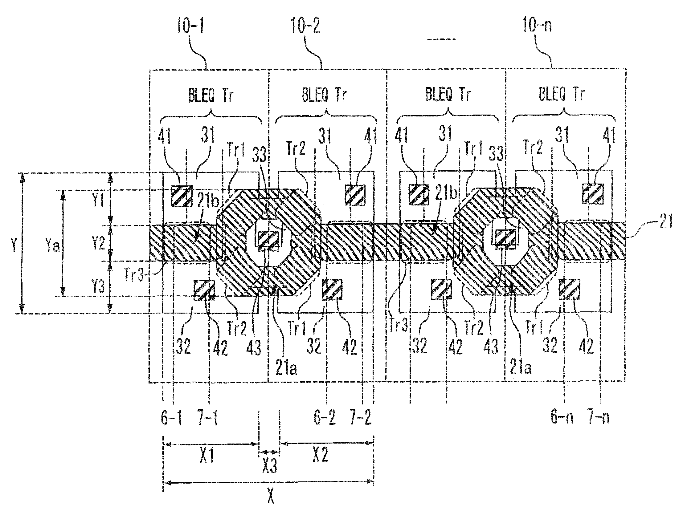
[0046]A semiconductor memory device in an exemplary embodiment of the present invention is provided with at least a memory cell and a sense amplifier for reading date from the memory cell, and is a semiconductor memory device, such as a DRAM, an SRAM (static random access memory), a flash memory and the like. A semiconductor memory device of this exemplary embodiment is installed in a computer provided with a CPU and a clock generation circuit. Although the following description will be given on the assumption that the semiconductor memory device is a DRAM, it is needless to say that the present invention can be applied also to a semiconductor memory device other than a DRAM.

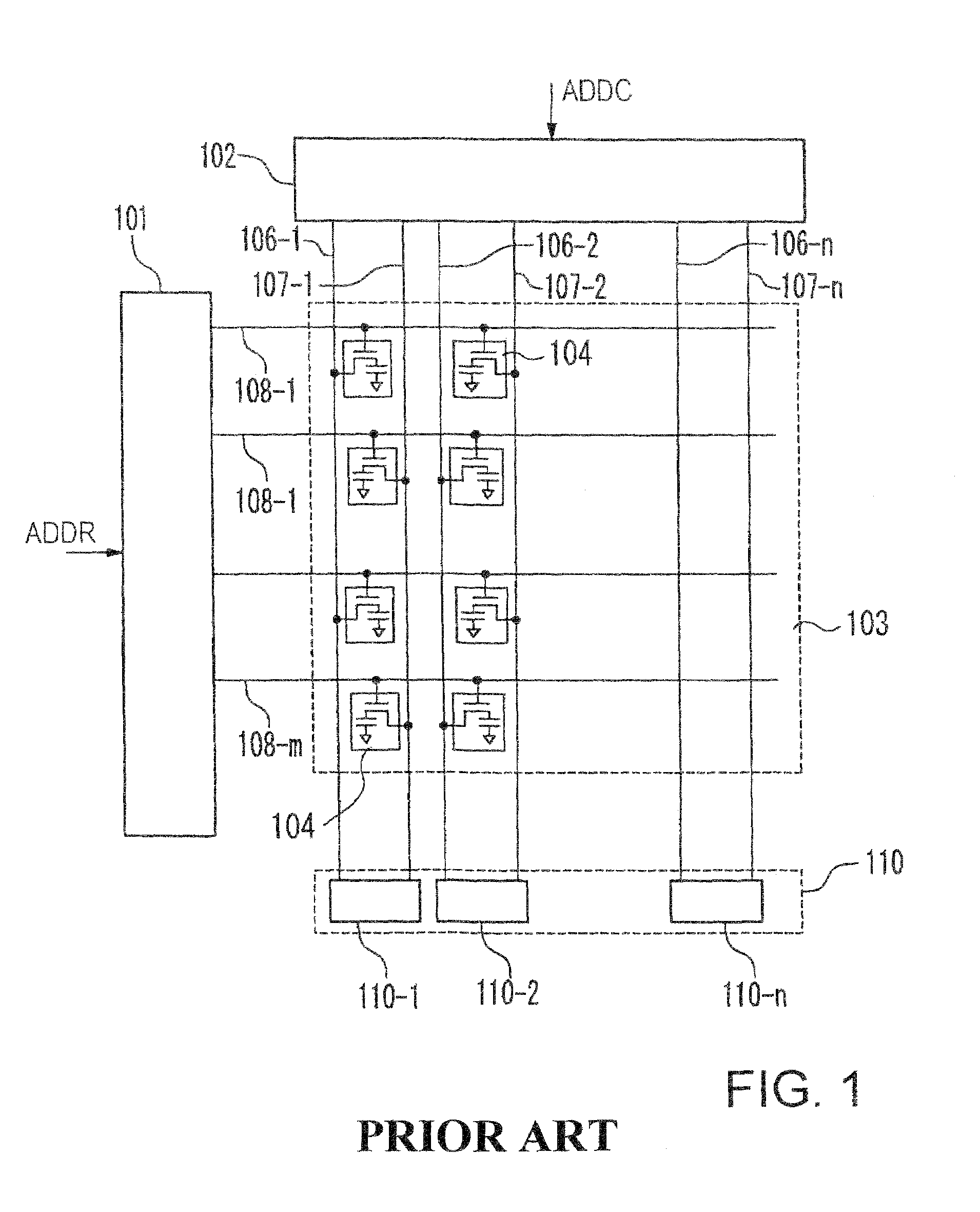
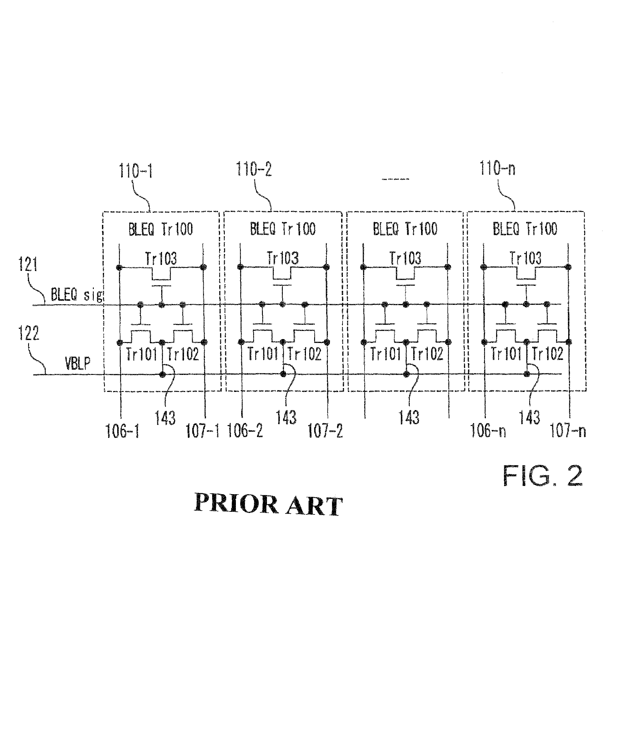
[0047]FIG. 5 shows the configuration of a semiconductor memory device of this embodiment. This semiconductor memory device is provided with m word lines 8-1 to 8-m, mb redundancy word lines 8b-1 to 8b-mb, n sets of bit line pairs, word driver 1 that drives the word lines and the redundancy word lines, data drive...


PUM


Abstract

In a sense amplifier circuit having a plurality of sense amplifier portions arranged in order, each of the sense amplifier portions includes a transistor that supplies a bit line potential to a bit line pair in a corresponding column of a memory cell array and a gate electrode for supplying a precharge signal to a gate of the transistor. The gate electrode of the plurality of sense amplifier portions is provided as one piece as a whole and extends in a direction parallel to a row direction in the memory cell array. A gate electrode portion which is a connected portion between the gate electrode in a k-th sense amplifier portion and the gate electrode in a (k+1)-th sense amplifier portion is ring-shaped, where k is an odd number.

Description

BACKGROUND OF THE INVENTION[0001]1. Field of the Invention[0002]The present invention relates to a semiconductor memory device and, more particularly, to a sense amplifier circuit provided within a semiconductor memory device.[0003]2. Description of the Related Arts[0004]In recent years, semiconductor memory devices exemplified by DRAMs (dynamic random access memories) have been developed on the basis of the use of leading-edge semiconductor device manufacturing processes and the scaledown of semiconductor memory devices is being carried out. In semiconductor memory devices, the size of a memory cell region is changing in the direction of shrinkage due to the ongoing scaledown in fabrication processes of the semiconductor devices. However, the scaledown as viewed form the standpoint of the whole semiconductor memory device has not been going on compared to the scaledown in the memory cell region and, for this reason, the shrinkage of the size of circuits provided in what is called a...

Claims


Application Information

Patent Timeline
Patent Type & Authority Patents(United States)
IPC IPC(8): G11C7/02
CPCG11C11/4091G11C11/4094G11C11/413G11C11/412H01L27/10897H10B12/50
Inventor OHGAMI, TAKESHI
Owner LONGITUDE SEMICON S A R L
Why Eureka
Try Eureka