Carrier sheet with adhesive film and method for producing semiconductor devices using the carrier sheet with adhesive film

a carrier sheet and adhesive film technology, applied in the direction of film/foil adhesives, heat-activated film/foil adhesives, solid-state devices, etc., can solve the problem of not so great adhesive effect of film, and achieve the effect of higher degree of crosslinking of polymer chains

Active Publication Date: 2009-09-08
INTEL CORP
View PDF8 Cites 1 Cited by
  • Summary
  • Abstract
  • Description
  • Claims
  • Application Information

AI Technical Summary

Benefits of technology

[0008]One advantage of this carrier sheet with adhesive film is that the deactivated regions of the adhesive layer on the upper side no longer enter into interaction with a plastic package molding compound, so that the carrier sheet with the adhesive film can be removed from the forming coplanar upper side, comprising upper sides of the semiconductor chips and the surface of the plastic package molding compound, without leaving any residual material behind. At the same time, however, the adhesive effect of the adhesive layer with respect to the semiconductor chips is obtained, so that the latter retain their position on the carrier sheet when the plastic package molding compound is applied.
[0009]Another advantage of this carrier sheet with adhesive film is consequently that partial regions of the upper side of the adhesive film are deactivated and no longer exhibit any adhesive effect, while the regions which are intended to have the adhesive effect under the semiconductor chips continue as before to produce the full adhesive effect. Nevertheless, the adhesive effect of the film is not so great that, after they become embedded in the plastic package molding compound, the semiconductor chips can be torn out from the plastic package molding compound. Instead, the adhesive effect of the adhesive film is still sufficient to keep the semiconductor chips in position for embedding in a plastic package molding compound or for forming a panel, but it is not so great that, when the adhesive film is removed, the semiconductor chips can be torn out from the cooled-down plastic package molding compound.
[0012]In a further exemplary embodiment of the invention, the deactivated regions of the adhesive layer have a higher degree of crosslinking of polymer chains than the actively adhesive regions under the semiconductor chips. This higher degree of crosslinking of the polymer chains may be achieved by high-energy irradiation of the adhesive layer and an associated premature artificial aging. The adhesive layer is thereby prematurely cured and its adhesive effect in relation to a plastic package molding compound is reduced accordingly.
[0017]Independently of the production of the semiconductor chips, a carrier sheet for a panel is produced, the upper side of the carrier including a double-sided adhesive film with a film underside and a film upper side. The film underside is adhesively fixed on the carrier sheet, and the upper side remains freely accessible, and includes semiconductor device positions arranged in rows and columns. Next, this carrier sheet with the double-sided adhesive film is loaded with the individual semiconductor chips from the freely accessible film upper side, the individual semiconductor chips being arranged with their active upper sides on the film upper side of the adhesive film in the respective semiconductor device positions. After loading, a deactivation of the freely accessible film upper side takes place, thereby reducing the adhesive effect of the freely accessible film upper side.
[0019]One advantage of the method of the invention is that, due to the deactivation of the freely accessible film upper side, a smooth, coplanar upper side is produced in the region of the plastic package molding compound. This upper side can be covered directly with a wiring structure, for example, comprising a copper coating, without the occurrence of planarity problems.

Problems solved by technology

Nevertheless, the adhesive effect of the film is not so great that, after they become embedded in the plastic package molding compound, the semiconductor chips can be torn out from the plastic package molding compound.

Method used


Image

  • Carrier sheet with adhesive film and method for producing semiconductor devices using the carrier sheet with adhesive film
  • Carrier sheet with adhesive film and method for producing semiconductor devices using the carrier sheet with adhesive film
  • Carrier sheet with adhesive film and method for producing semiconductor devices using the carrier sheet with adhesive film

Examples


Embodiment Construction

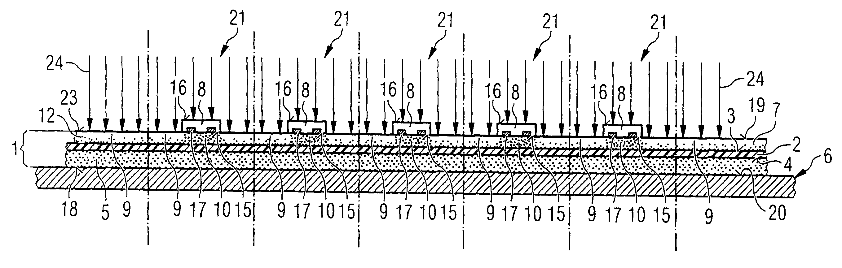
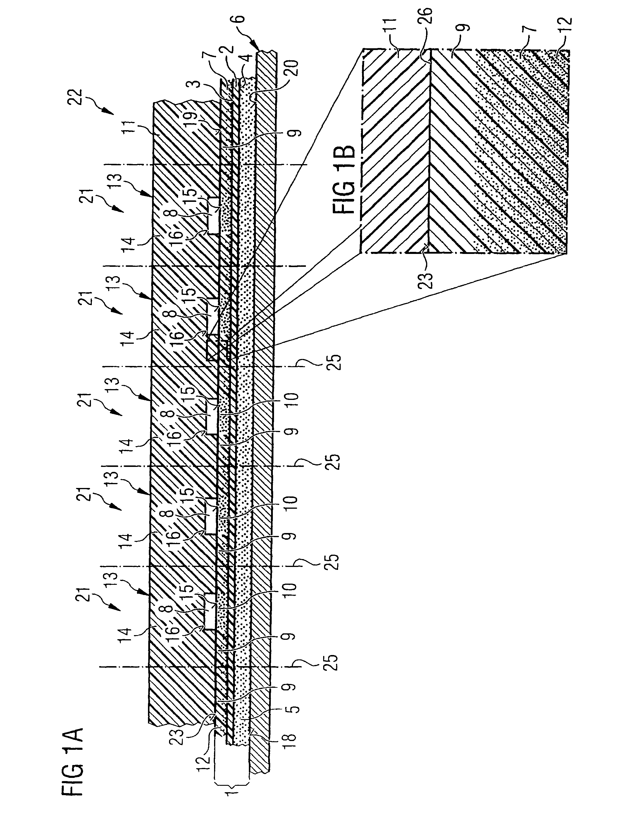
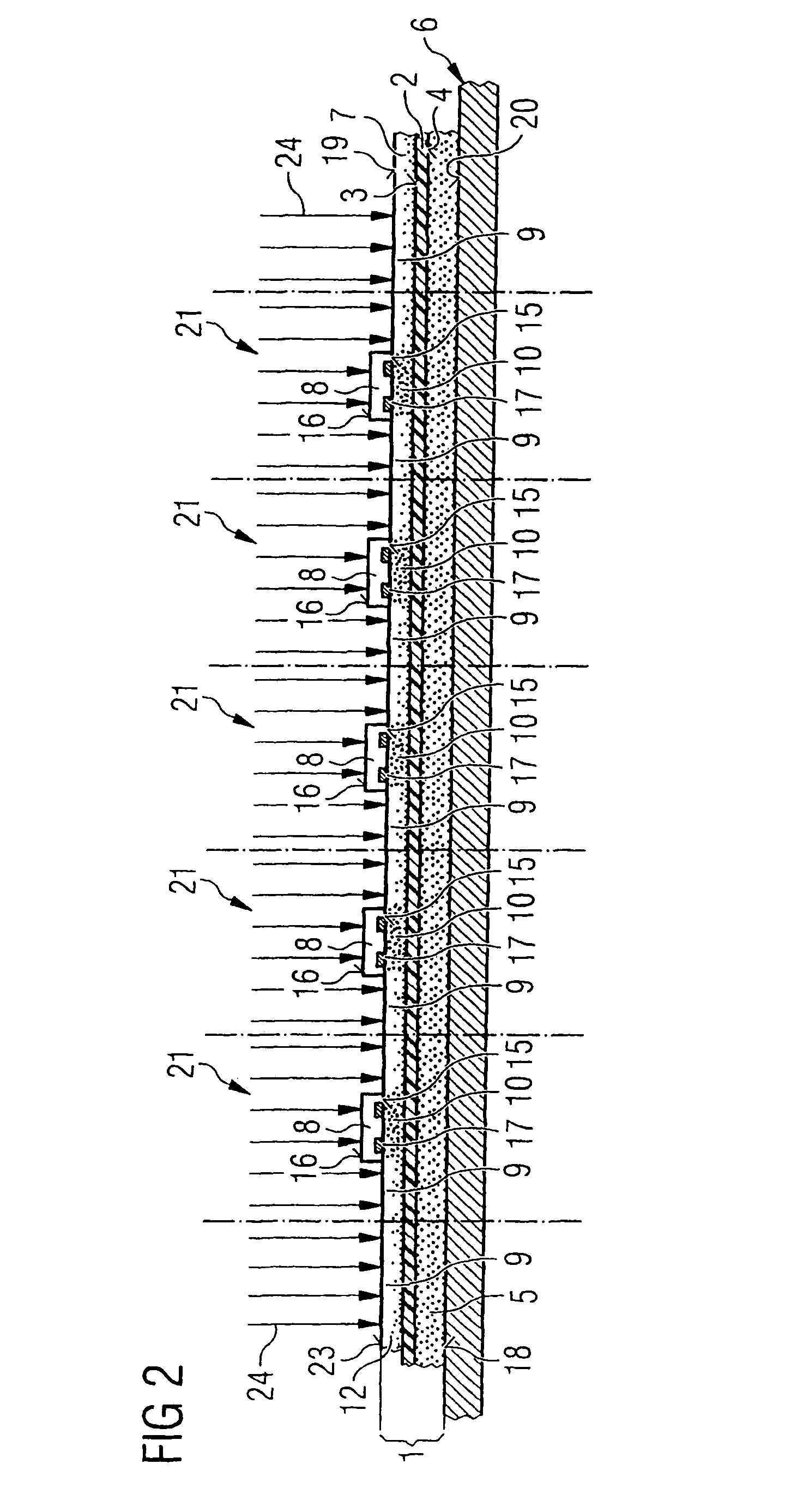
[0029]FIG. 1A shows a schematic cross-section of a panel 22 on a carrier sheet 6 with adhesive film 1, according to one embodiment of the invention. The panel 22 includes a number of semiconductor device positions 21, which are arranged in columns and rows, in this cross-section only dash-dotted lines 25 showing the series arrangement of the semiconductor device positions 21 with their plastic packages 14. A semiconductor device 13 is arranged in each of the semiconductor device positions 21 shown here, all the semiconductor devices 13 of the panel 22 being held by the common carrier sheet 6 in this state of prefabrication. This carrier sheet 6 is loaded with the adhesive film 1, which includes a base film 2, which is preferably produced from a thermally resistant PET material.

[0030]The underside 4 of the base film 2 includes a thermoactive adhesive layer 5, by which the double-sided adhesive film 1 is connected to the carrier upper side 18 of the carrier sheet 6. The upper side 18 ...


PUM

PropertyMeasurementUnit
adhesiveaaaaaaaaaa
heat-resistantaaaaaaaaaa
pressure-sensitiveaaaaaaaaaa

Abstract

A carrier sheet with an adhesive film includes a heat-resistant base film with an upper side and an underside, and a thermoactive adhesive layer arranged on the underside of the base film and oriented toward the carrier sheet. The upper side of the base film includes an adhesive layer with semiconductor chips fixed on it, the semiconductor chips being surrounded by deactivated regions of the adhesive layer of the film upper side.

Description

CROSS REFERENCE TO RELATED APPLICATIONS[0001]This application claims priority under 35 USC §119 to German Application No. DE 10 2005 024 431.9, filed on May 24, 2005, and titled “Carrier Sheet with Adhesive Film and Method for Producing Semiconductor Devices Using the Carrier Sheet with Adhesive Film,” the entire contents of which are hereby incorporated by reference.FIELD OF THE INVENTION[0002]The invention relates to a carrier sheet with adhesive film that includes a heat-resistant base film.BACKGROUND[0003]Double-sided adhesive films which can be positioned on corresponding carrier sheets are known in the art and are used variously in semiconductor technology. However, a particular problem arises if such adhesive films come into contact with plastic package molding compounds and form a common boundary surface. It is found in this case that the double-sided adhesive films have an undesirably strong adhesion in relation to the molding compound. This adhesion may be attributable to ...

Claims


Application Information

Patent Timeline
Patent Type & Authority Patents(United States)
IPC IPC(8): H01L21/00C09J7/35
CPCC09J7/0203H01L21/561H01L21/568H01L21/67132H01L24/96C09J7/0217H01L2924/01029C09J2201/134C09J2201/28C09J2203/326C09J2427/006C09J2433/00C09J2467/006H01L21/67126H01L2221/68318H01L2924/181H01L2924/14C09J7/35C09J7/385C09J2301/1242C09J2301/204H01L2924/00
Inventor BEER, GOTTFRIEDBRUNNBAUER, MARKUSESCHER-POEPPEL, IRMGARDFUERGUT, EDWARD
Owner INTEL CORP
Why Eureka
Try Eureka