
Method of forming transistor devices with different threshold voltages using halo implant shadowing

a technology of halo implants and transistor devices, applied in the field of method, can solve the problems of increased manufacturing time, increased manufacturing cost, and additional process complexity, and achieve the effect of reducing the number of implant masking steps

Active Publication Date: 2009-10-06
TAIWAN SEMICON MFG CO LTD
View PDF6 Cites 1 Cited by
  • Summary
  • Abstract
  • Description
  • Claims
  • Application Information

AI Technical Summary

Benefits of technology

This approach enables the production of semiconductor transistor devices with varying threshold voltages on a single wafer, reducing the number of implant masking steps and simplifying the manufacturing process while maintaining control over doping levels and energies.

Problems solved by technology

The use of multiple implant masks in this manner results in increased manufacturing cost, additional process complexity, and increased manufacturing time.

Method used


Image

  • Method of forming transistor devices with different threshold voltages using halo implant shadowing
  • Method of forming transistor devices with different threshold voltages using halo implant shadowing
  • Method of forming transistor devices with different threshold voltages using halo implant shadowing

Examples


Embodiment Construction

[0017]The following detailed description is merely illustrative in nature and is not intended to limit the embodiments of the invention or the application and uses of such embodiments. For the sake of brevity, conventional techniques related to semiconductor device fabrication may not be described in detail herein. Moreover, the various tasks and process steps described herein may be incorporated into a more comprehensive procedure or process having additional steps or functionality not described in detail herein. In particular, various steps in the manufacture of semiconductor transistor devices are well known and so, in the interest of brevity, many conventional steps will only be mentioned briefly herein or will be omitted entirely without providing the well known process details.

[0018]The techniques and technologies described herein may be utilized to fabricate MOS transistor devices, including NMOS transistor devices, PMOS transistor devices, and CMOS transistor devices. Althou...


PUM


Abstract

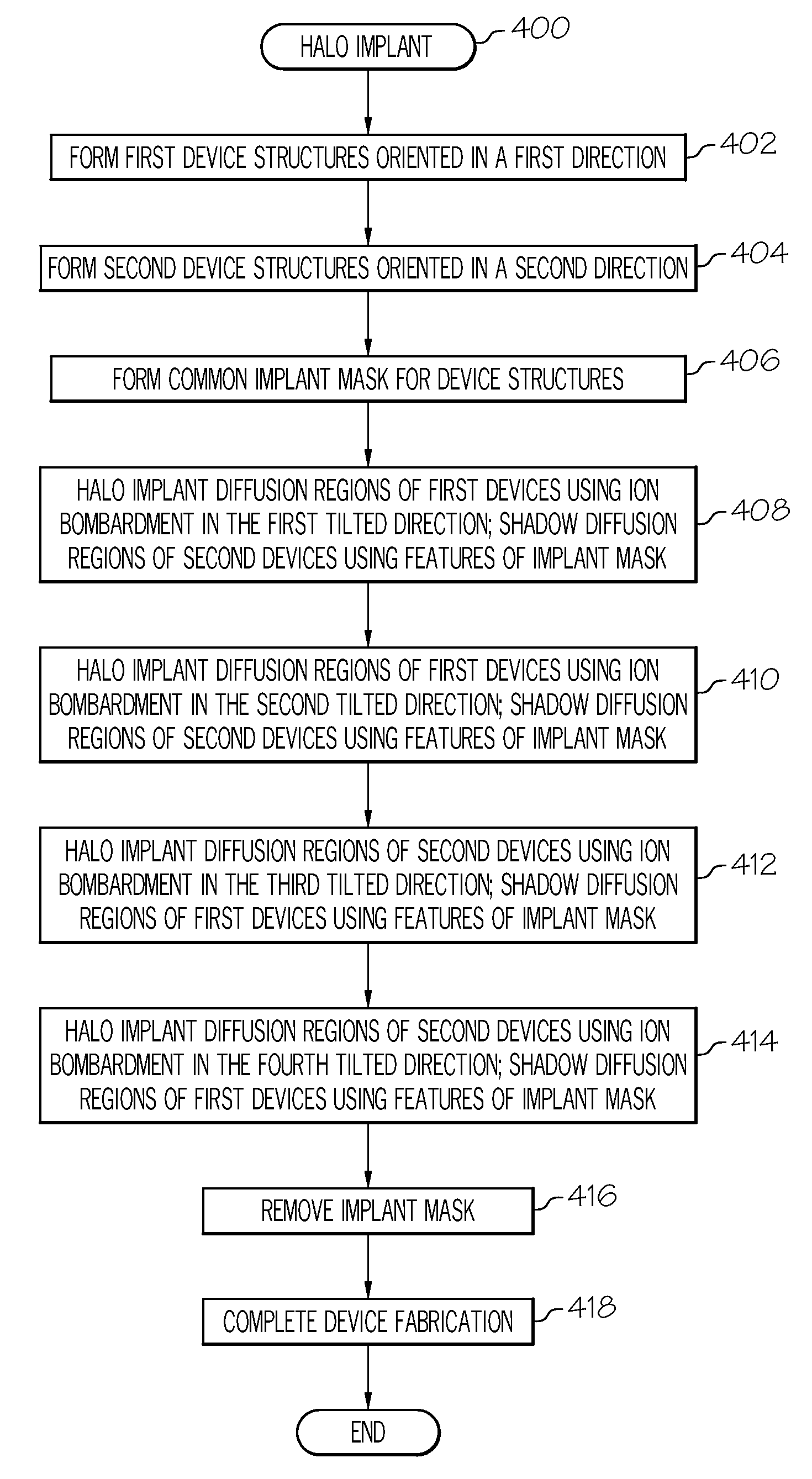
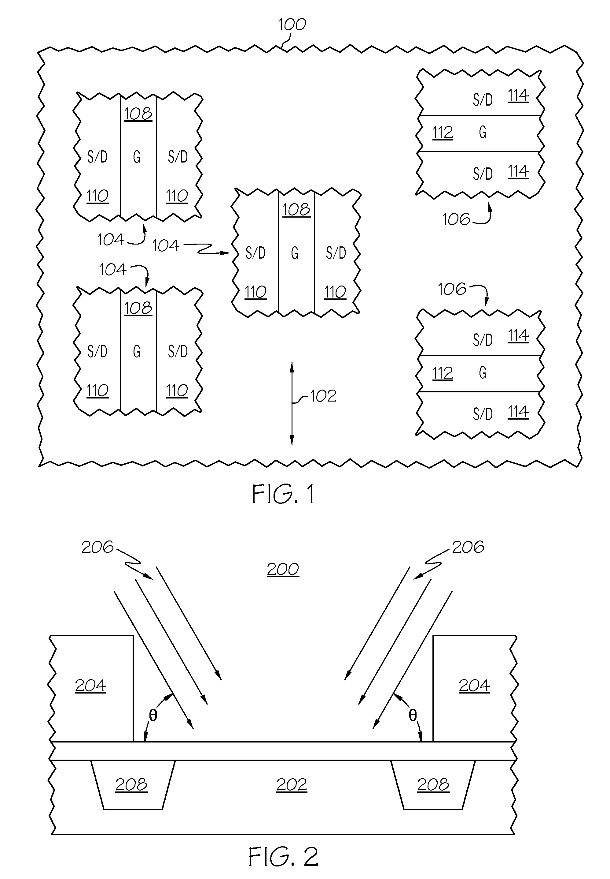
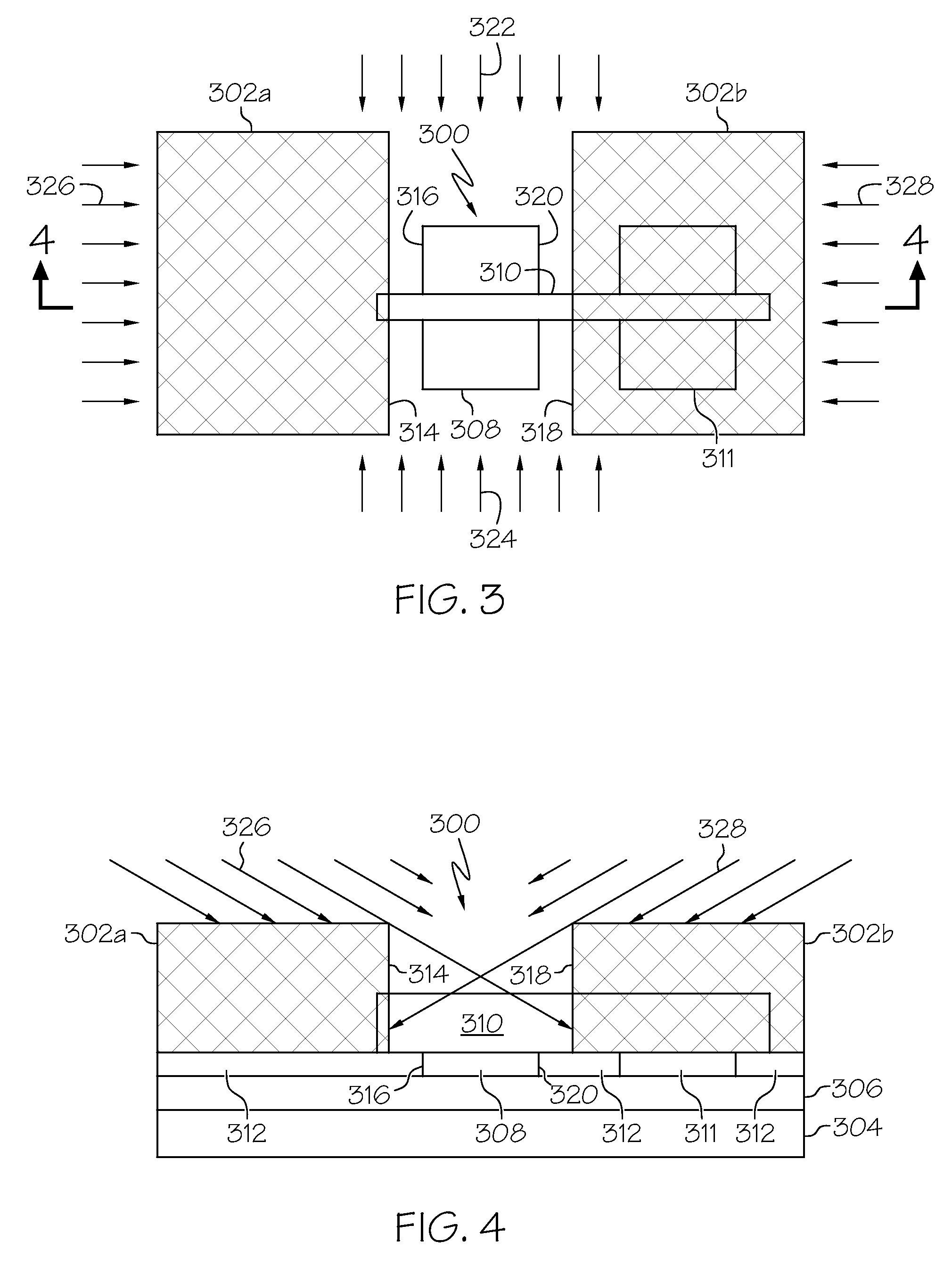
The halo implant technique described herein employs a halo implant mask that creates a halo implant shadowing effect during halo dopant bombardment. A first transistor device structure and a second transistor device structure are formed on a wafer such that they are orthogonally oriented to each other. A common halo implant mask is created with features that prevent halo implantation of the diffusion region of the second transistor device structure during halo implantation of the diffusion region of the first transistor device structure, and with features that prevent halo implantation of the diffusion region of the first transistor device structure during halo implantation of the diffusion region of the second transistor device structure. The orthogonal orientation of the transistor device structures and the pattern of the halo implant mask obviates the need to create multiple implant masks to achieve different threshold voltages for the transistor device structures.

Description

TECHNICAL FIELD[0001]Embodiments of the subject matter described herein relate generally to semiconductor device manufacturing. More particularly, embodiments of the subject matter relate to the use of halo implants during the fabrication of semiconductor transistor devices.BACKGROUND[0002]Semiconductor transistor devices and related manufacturing processes are well known. Ion implants in the channel regions of a semiconductor transistor device are utilized to obtain the desired device threshold voltage. Before ions are implanted in the channel regions, an implant mask is patterned on the wafer to protect certain areas from becoming implanted with the ions. Halo implants, which are doped regions formed by bombarding the semiconductor wafer with tilted beams of ions, are often used during the manufacture of semiconductor transistor devices.[0003]It is desirable, from a design flexibility standpoint, to create a semiconductor device having transistors characterized by different thresh...

Claims


Application Information

Patent Timeline
Patent Type & Authority Patents(United States)
IPC IPC(8): H01L21/425
CPCH01L21/26513H01L29/1083H01L21/823807H01L21/26586
Inventor ZHOU, JINGRONGMICHAEL, MARKMICHAEL, LEGAL REPRESENTATIVE, DONNAWUBULLER, JAMES F.SULTAN, AKIF
Owner TAIWAN SEMICON MFG CO LTD
Learn More