Semiconductor chip and semiconductor integrated circuit device for relaying a reference clock from one hard macro to another

a semiconductor integrated circuit and reference clock technology, applied in the direction of generating/distributing signals, digital data processing details, instruments, etc., can solve the problems of data communication reliability degradation, reduce the number of reference clock wirings, reduce interconnection capacity, and improve routing performance

Active Publication Date: 2009-10-13
RENESAS ELECTRONICS CORP
View PDF4 Cites 3 Cited by
  • Summary
  • Abstract
  • Description
  • Claims
  • Application Information

AI Technical Summary

Benefits of technology

[0015]Therefore, when a package in which the semiconductor chip is encapsulated is mounted on a board, only one package pin is sufficient to input the reference clock into the semiconductor chip. The one package pin is connected to a clock pad of the semiconductor chip. The reference clock is supplied from one reference clock wiring on the board to the above-mentioned one hard macro through the one package pin and the clock pad. As described above, it is possible according to the present invention to reduce the number of reference clock wirings on the board even when the plurality of hard macros are provided in one semiconductor chip. Thus, routing performance is improved, and interconnection capacity is reduced.

Problems solved by technology

If noises and jitters are mixed into the reference clock CLK, reliability of the data communication deteriorates due to the increase in error rate.

Method used


Image

  • Semiconductor chip and semiconductor integrated circuit device for relaying a reference clock from one hard macro to another
  • Semiconductor chip and semiconductor integrated circuit device for relaying a reference clock from one hard macro to another
  • Semiconductor chip and semiconductor integrated circuit device for relaying a reference clock from one hard macro to another

Examples


first embodiment

Circuit Configuration

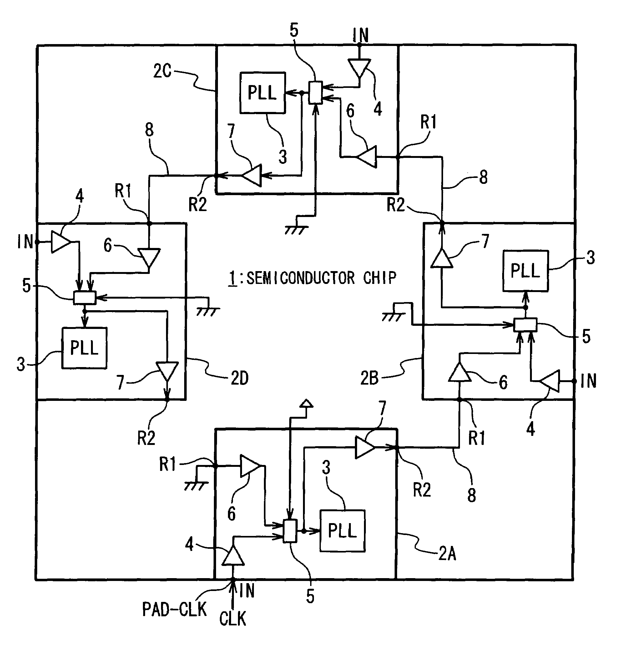
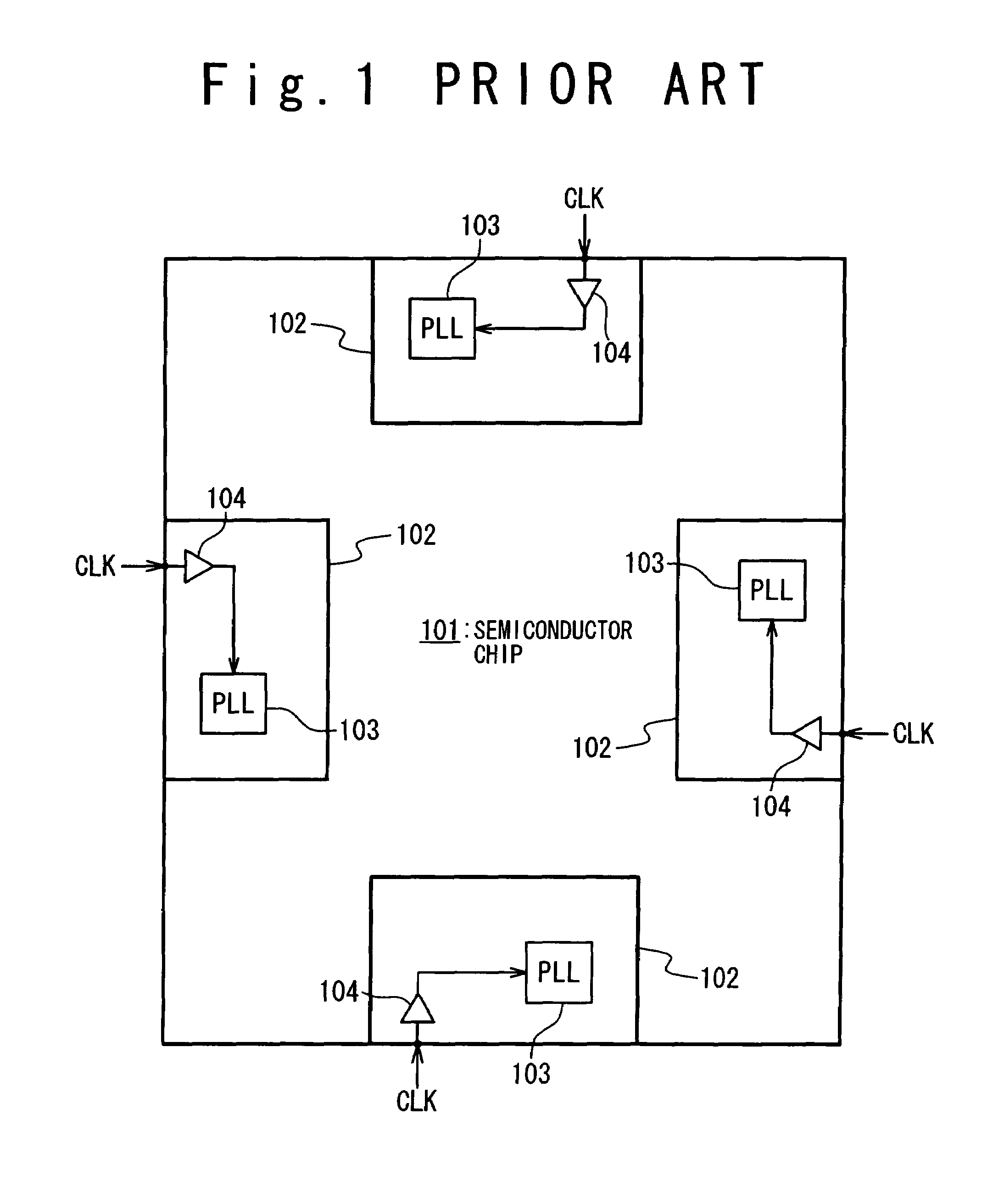
[0024]FIG. 3 is a circuit block diagram schematically showing a configuration of a semiconductor chip 1 according to a first embodiment of the present invention. In the semiconductor chip 1 shown in FIG. 3, a plurality of hard macros 2A to 2D are provided next to four sides of the chip, respectively.

[0025]Each of the hard macros 2A to 2D is configured to operate on the basis of a reference clock CLK that is supplied to the semiconductor chip 1 from the outside. More particularly, each hard macro 2 includes a PLL circuit 3 which multiplies the input reference clock CLK to generate a high-speed clock. The high-speed clock generated by the PLL circuit 3 is supplied to a signal processing circuit (not shown). The signal processing circuit performs a predetermined operation on the basis of the high-speed clock.

[0026]For example, each hard macro 2 is a serializer / deserializer (SerDes) macro for executing serial-parallel conversion of data. In this case, the PLL circui...

second embodiment

Circuit Configuration

[0038]FIG. 5 is a circuit block diagram schematically showing a configuration of a semiconductor chip 1′ according to a second embodiment of the present invention. In FIG. 5, the same reference numerals are given to the same components as those described in the first embodiment, and the redundant description will be appropriately omitted. In the semiconductor chip 1′ shown in FIG. 5, a plurality of hard macros 2E to 2H are provided next to four sides of the semiconductor chip 1′, respectively.

[0039]Each hard macro 2 is provided with a clock input terminal IN, a first relay input terminal R1a, a second relay input terminal R1b, a first relay output terminal R2a and a second relay output terminal R2b. The first relay input terminal R1a and the first relay output terminal R2a are provided on the same side (a first side) of the hard macro 2. The second relay input terminal R1b and the second relay output terminal R2b are provided on the same side (a second side) of ...

third embodiment

Circuit Configuration

[0052]FIG. 6 is a circuit block diagram schematically showing a configuration of a semiconductor chip 1″ according to a third embodiment of the present invention. In FIG. 6, the same reference numerals are given to the same components as those described in the first embodiment, and the redundant description will be appropriately omitted. In FIG. 6, the same hard macro 2 as in the first embodiment is used. It goes without saying that the same hard macro 2 as in the second embodiment can be used.

[0053]In the semiconductor chip 1″ shown in FIG. 6, a relay hard macro 20 is provided between the hard macro 2A and the hard macro 2C. The relay hard macro 20 plays a role of relaying the reference clock CLK between the hard macros 2A and 2C. More specifically, the relay hard macro 20 has the relay input terminal R1, the relay output terminal R2 and a relay buffer 21. An input of the relay buffer 21 is connected to the relay input terminal R1, and an output thereof is conn...


PUM


Abstract

A semiconductor chip has: a plurality of hard macros which operates based on a reference clock; and a clock pad through which the reference clock is supplied from the outside to one of the plurality of hard macros. The reference clock supplied to the one hard macro is relayed to other hard macros of the plurality of hard macros in order.

Description

BACKGROUND OF THE INVENTION[0001]1. Field of the Invention[0002]The present invention relates to a semiconductor chip and a semiconductor integrated circuit device. Particularly, the present invention relates to a technique of clock supplying in a semiconductor chip and a semiconductor integrated circuit device.[0003]2. Description of the Related Art[0004]Demand for a high-performance computer server and a high-performance network device is increasing so as to realize a next-generation broadband network which serves as a foundation for an advanced IT society. It is essential for the high-performance computer server and the high-performance network device to execute high-speed transfer of data between LSIs. As a high-speed communication method, a serial communication method has become mainstream, in which one transmission line is used for transmitting data so as to avoid the burden of controlling the timing between data.[0005]In the serial communication, a device for converting paral...

Claims


Application Information

Patent Timeline
Patent Type & Authority Patents(United States)
IPC IPC(8): G06F1/00G06F1/04G06F1/12G06F17/50
CPCG01R31/31715G01R31/318547G01R31/31727
Inventor FURUYA, NOBUO
Owner RENESAS ELECTRONICS CORP
Why Eureka
Try Eureka