Systems and methods for improved scan testing fault coverage

a scan test and fault coverage technology, applied in the field of test methods, can solve the problems of not providing the simple result of the logic circuit either, affecting the proper operation of the device, and specific and improbable combinations, etc., and achieve the effect of improving the fault coverage of scan tests

Inactive Publication Date: 2009-10-20
TOSHIBA AMERICA ELECTRONICS COMPONENTS
View PDF11 Cites 10 Cited by
  • Summary
  • Abstract
  • Description
  • Claims
  • Application Information

AI Technical Summary

Problems solved by technology

As digital devices (e.g., integrated circuits) have become more complex and more densely packed with logic gates and other electronic components, there are more and more opportunities for manufacturing defects to occur, thereby impairing or impeding the proper operation of the devices.
Because the use of pseudorandom patterns is not deterministic (i.e., it does not test each and every possible combination of inputs, states and outputs), it does not provide the simple result that the logic circuit either does or does not have any defects.
Some components or portions of the circuitry, however, may require a very specific and improbable combination of bits to properly test the circuitry.
Because this is unlikely in a pseudorandom sequence of bits, it gives rise to concerns regarding the likelihood that all output states will be exercised during testing.
While it might at first appear to be possible to provide additional logic between the scan latches and the target logic to be tested in order to force the inputs to the target logic to desired values, this may violate timing constraints of the LBIST and / or target logic.
Placing additional logic between the scan latches and the many-input AND gate may therefore not allow enough time for the data to propagate from the scan latches to the output of the many-input AND gate, causing errors in the testing.

Method used


Image

  • Systems and methods for improved scan testing fault coverage
  • Systems and methods for improved scan testing fault coverage
  • Systems and methods for improved scan testing fault coverage

Examples


Embodiment Construction

[0026]One or more embodiments of the invention are described below. It should be noted that these and any other embodiments described below are exemplary and are intended to be illustrative of the invention rather than limiting.

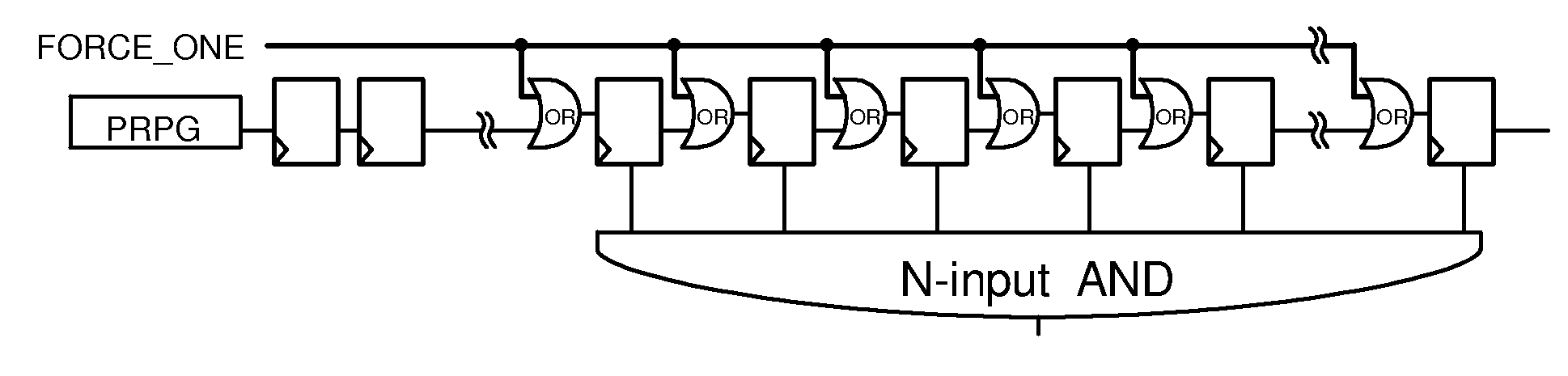
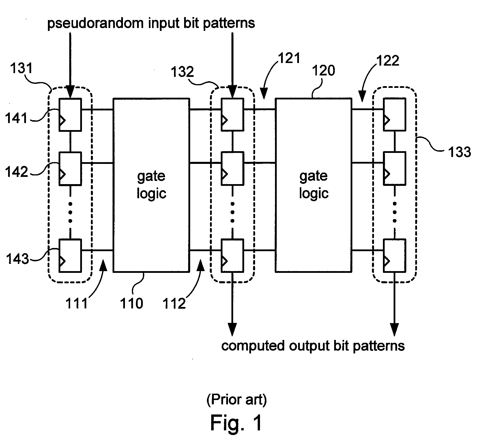
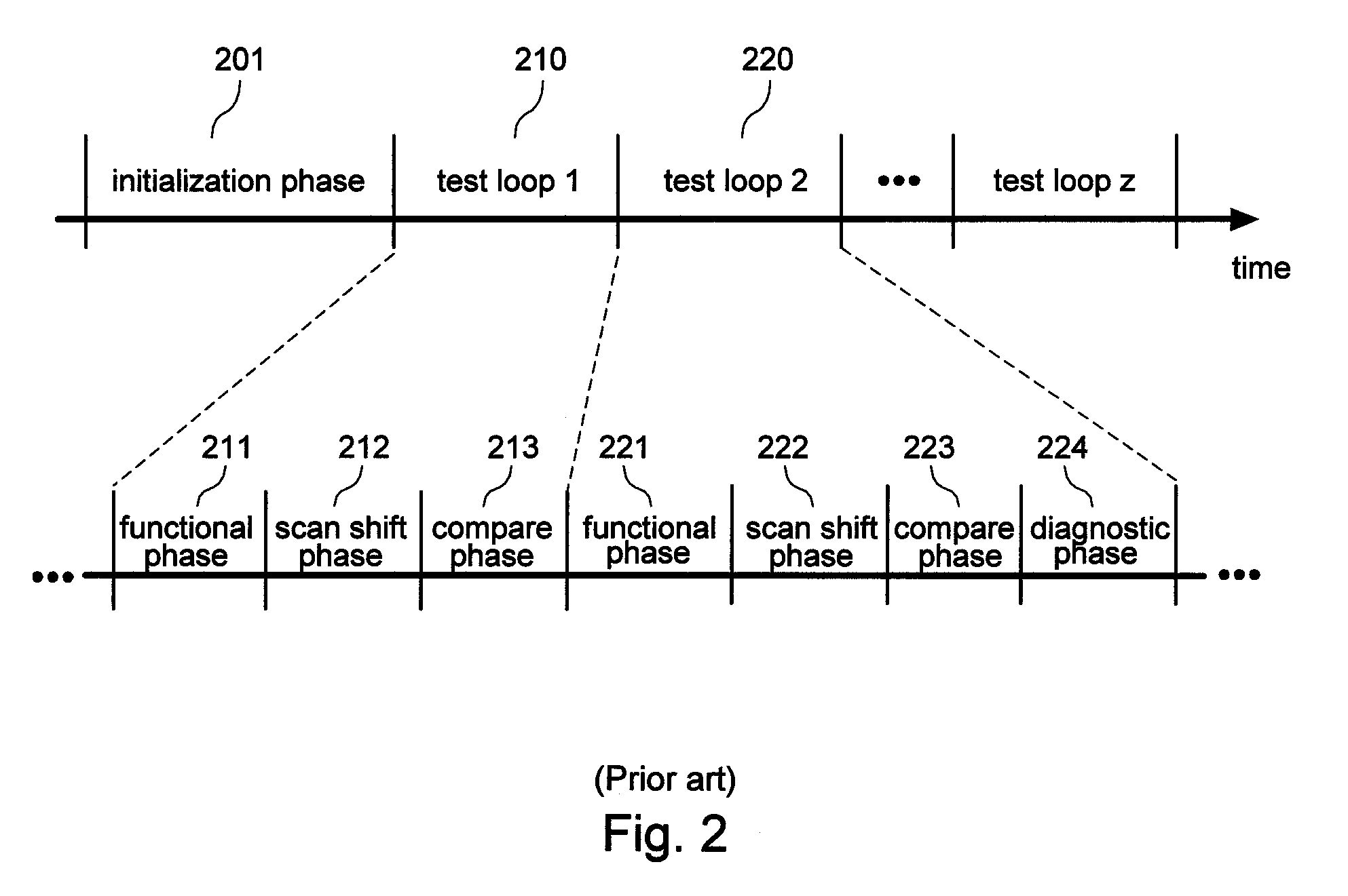
[0027]As described herein, various embodiments of the invention comprise systems and methods associated with integrated circuits (ICs) to manage the composition of input test bit patterns to improve the fault coverage of scan tests such as logic built-in-self-tests (LBISTs). While the embodiments described in detail below are implemented in LBIST systems, it should be noted that alternative embodiments may be implemented in systems that implement testing using automated test pattern generators (ATPG's) or other means to generate test patterns for the scan chains. References below to LBIST should therefore be construed broadly to encompass ATPG-based systems and other types of test systems that use scan chains.

[0028]The various embodiments of the invention may...


PUM


Abstract

Systems and methods for improved fault coverage of logic built-in-self-tests (LBISTs) in integrated circuits (ICs) which ensure testing of specific logic by forcing specific values into scan latches that contain otherwise pseudorandom test bit patterns. In one embodiment, an LBIST system comprises a plurality of scan latches and forcing logic coupled to a first set of the scan latches which provide inputs to selected target logic. The forcing logic is configured to overwrite values stored in the first set of scan latches with desired values. In one embodiment, the forcing logic includes a bypass path that enables shifting of unaltered bit patterns around the first set of scan latches. Bits in the bypass path may be inverted when the bypass path is not being used in order to help detect errors in the operation of the bypass path.

Description

BACKGROUND[0001]1. Field of the Invention[0002]The invention relates generally to test methods, and more particularly to systems and methods for providing improved fault coverage of scan tests, such as logic built-in-self-tests, in integrated circuits by controlling the data passing through certain components.[0003]2. Related art[0004]As digital devices (e.g., integrated circuits) have become more complex and more densely packed with logic gates and other electronic components, there are more and more opportunities for manufacturing defects to occur, thereby impairing or impeding the proper operation of the devices. Consequently, the testing of these devices is becoming increasingly important. With respect to the testing of devices, and more particularly manufactured integrated circuits (ICs), one mechanism that is very useful is a built-in self test (BIST). This may also be referred to as a logic built-in self test (LBIST).[0005]BIST and LBIST methodologies are generally considered...

Claims


Application Information

Patent Timeline
Patent Type & Authority Patents(United States)
IPC IPC(8): G01R31/28
CPCG01R31/318342G01R31/318547G01R31/318544
Inventor OSANAI, TAKEKI
Owner TOSHIBA AMERICA ELECTRONICS COMPONENTS
Why Eureka
Try Eureka