
Integrated circuit with increased fault coverage

a technology of integrated circuits and fault coverage, applied in the direction of error detection/correction, cad circuit design, instruments, etc., can solve the problems of ics to malfunction, atpg does not have enough memory capacity to store an entire test set, and misses the ability to detect faults

Active Publication Date: 2016-03-29
NXP USA INC
View PDF13 Cites 16 Cited by
  • Summary
  • Abstract
  • Description
  • Claims
  • Application Information

AI Technical Summary

Benefits of technology

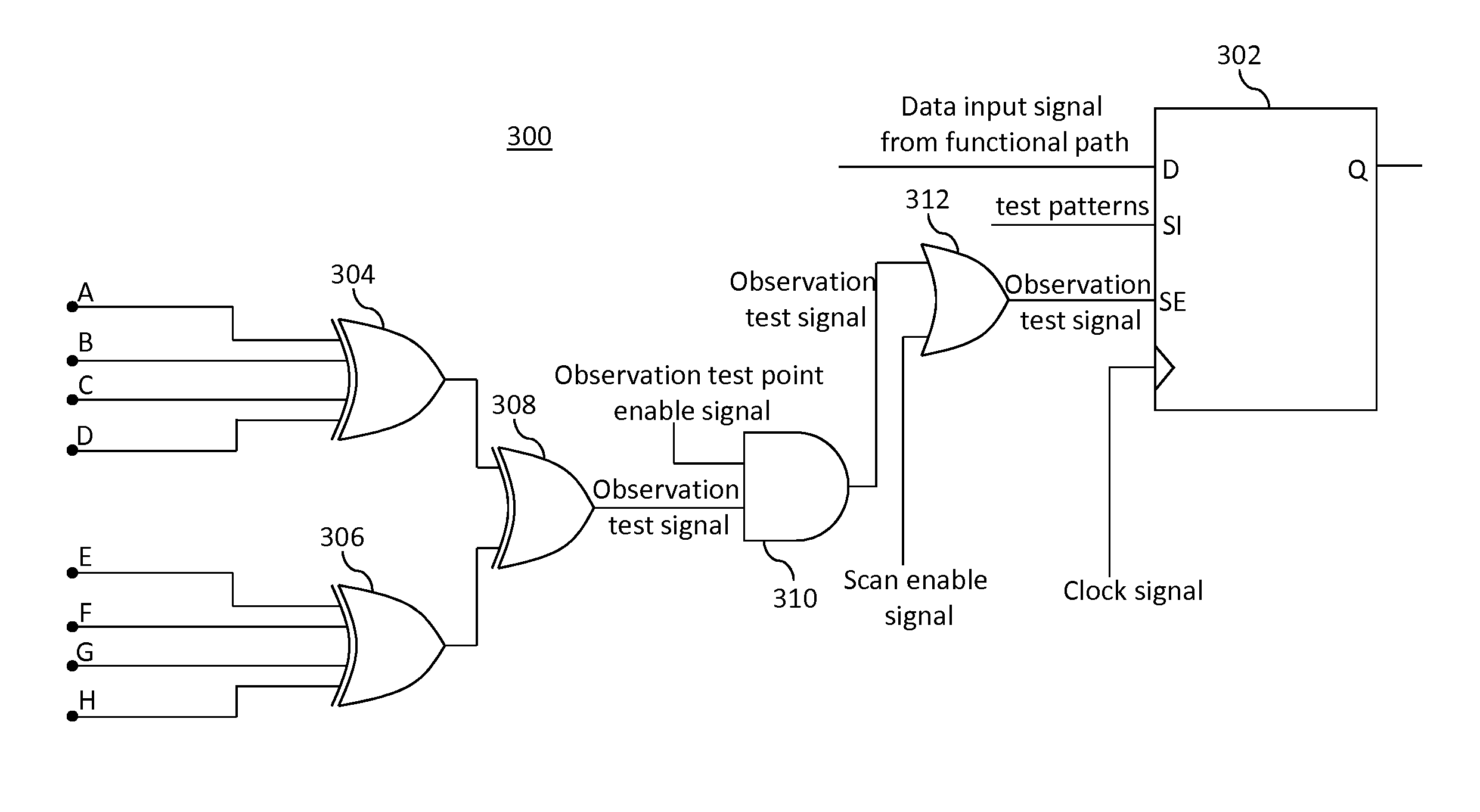
The present invention relates to an electronic design automation (EDA) tool for increasing the fault coverage of integrated circuits (ICs). The tool uses various techniques such as scan testing and built-in self-testing (BIST) to detect and locate manufacturing defects in ICs. The invention aims to improve the effectiveness and efficiency of fault testing during the design phase of an IC. The technical effect of the invention is to increase the reliability and accuracy of fault testing, which can help to reduce manufacturing costs and improve the overall quality of the IC.

Problems solved by technology

Such ICs may have manufacturing defects that are caused by dust particle contamination during fabrication, which can cause the ICs to malfunction.
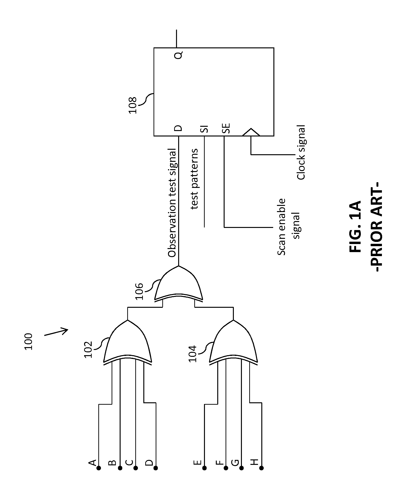
However, the ATPG does not have enough memory capacity to store an entire test set that covers all of the transition, path-delay, and stuck-at fault models.
However, the pseudo random test patterns that are applied to the CUT during BIST do not provide sufficient fault coverage and often miss hard to detect faults.
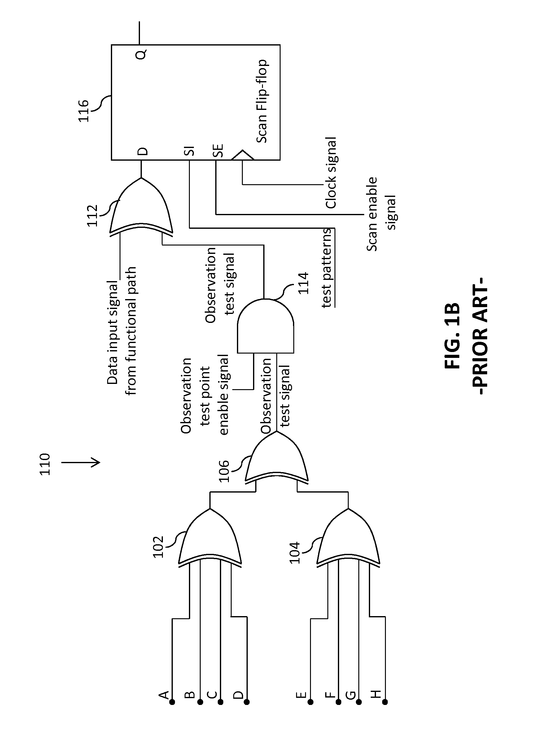
Therefore, the length of the scan paths increase, which increases the area overhead and the time required for testing the IC 100.
However, the fourth XOR gate 112 adds a delay to the functional timing of the IC 100 during functional mode of operation.

Method used


Image

  • Integrated circuit with increased fault coverage
  • Integrated circuit with increased fault coverage
  • Integrated circuit with increased fault coverage

Examples


Embodiment Construction

[0017]The detailed description of the appended drawings is intended as a description of the currently preferred embodiments of the present invention, and is not intended to represent the only form in which the present invention may be practiced. It is to be understood that the same or equivalent functions may be accomplished by different embodiments that are intended to be encompassed within the spirit and scope of the present invention. As used herein, the term multiplexer has been abbreviated as a mux.

[0018]In an embodiment of the present invention, an electronic design automation (EDA) tool for increasing the fault coverage of an integrated circuit design is provided. The integrated circuit design includes a plurality of observation test points corresponding to outputs of a plurality of logic elements of the integrated circuit design. The EDA tool includes a memory that stores the integrated circuit design and a processor that is in communication with the memory. The processor in...


PUM


Abstract

An electronic design automation (EDA) tool for increasing the fault coverage of an integrated circuit (IC) design includes a processor that inserts at least one XOR gate, an AND gate, an OR gate and a multiplexer between observation test points and an existing first scan flip-flop of the IC design. The XOR gate provides an observation test signal to the first scan flip-flop by way of the AND gate, the OR gate, and the multiplexer such that the observation test signal covers the presence of faults at the observation test points. The first scan flip-flop outputs a data input signal, a set of test patterns, and a first set of test signals based on the observation test signal to indicate whether the IC design is faulty or not. A testable IC that can be structurally tested is fabricated using the IC design.

Description

BACKGROUND OF THE INVENTION[0001]The present invention relates generally to electronic design automation (EDA) tools, and, more particularly, to an EDA tool for increasing fault coverage of an integrated circuit.[0002]Integrated circuits (ICs) often include various analog and digital components. Such ICs may have manufacturing defects that are caused by dust particle contamination during fabrication, which can cause the ICs to malfunction. Thus, testing the ICs to detect such manufacturing defects is very important. Design-for-test (DFT) techniques add testability features to the ICs to check for and identify manufacturing defects. DFT enables automatic-test-equipment (ATE) to execute various fault tests on the IC. The ATEs use test patterns generated by test pattern generators such as, automatic test pattern generators (ATPG), pseudo-random pattern generators (PRPG), and so on, to detect faults in the ICs. The ICs that undergo such fault tests are referred to as circuits under test...

Claims


Application Information

Patent Timeline
IPC IPC(8): G06F17/50G06F11/26G01R31/3177G06F11/27G06F11/263
CPCG01R31/3177G06F17/5045G06F11/27G06F11/261G06F17/5022G06F11/26G06F11/263G06F30/30G06F30/333G06F30/33
Inventor JINDAL, ANURAGDING, HUANGSHENGWANG, LING
Owner NXP USA INC
Learn More