Reducing resistivity in interconnect structures by forming an inter-layer

a technology of interconnect structure and resistivity, which is applied in the direction of semiconductor devices, semiconductor/solid-state device details, electrical apparatus, etc., can solve the problems of low resistivity of copper, low rc delay caused by resistance in the interconnect structure, and reduced dimensions of copper interconnects, so as to improve the resistivity of interconnect structures

Inactive Publication Date: 2009-11-03
TAIWAN SEMICON MFG CO LTD
View PDF14 Cites 14 Cited by
  • Summary
  • Abstract
  • Description
  • Claims
  • Application Information

AI Technical Summary

Benefits of technology

[0012]The advantageous features of the present invention include improved resistivity of interconnect structures of the integrated circuit and full compatibility with existing integrated circuit fabrication processes.

Problems solved by technology

Copper has low resistivity, thus the RC delay caused by the resistance in the interconnect structure is low.
However, with the scaling of integrated circuits, the dimensions of copper interconnects are also down-scaled.
As a result, the RC delay from the interconnect structure significantly increases.

Method used


Image

  • Reducing resistivity in interconnect structures by forming an inter-layer
  • Reducing resistivity in interconnect structures by forming an inter-layer
  • Reducing resistivity in interconnect structures by forming an inter-layer

Examples


Embodiment Construction

[0016]The making and using of the presently preferred embodiments are discussed in detail below. It should be appreciated, however, that the present invention provides many applicable inventive concepts that can be embodied in a wide variety of specific contexts. The specific embodiments discussed are merely illustrative of specific ways to make and use the invention, and do not limit the scope of the invention.

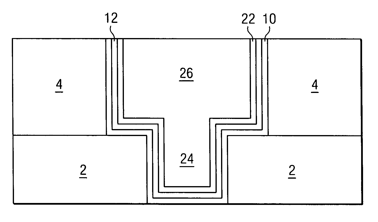
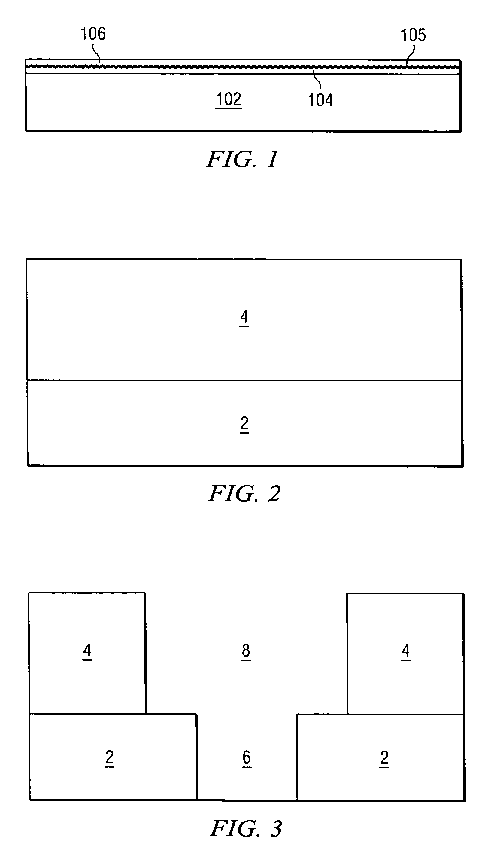
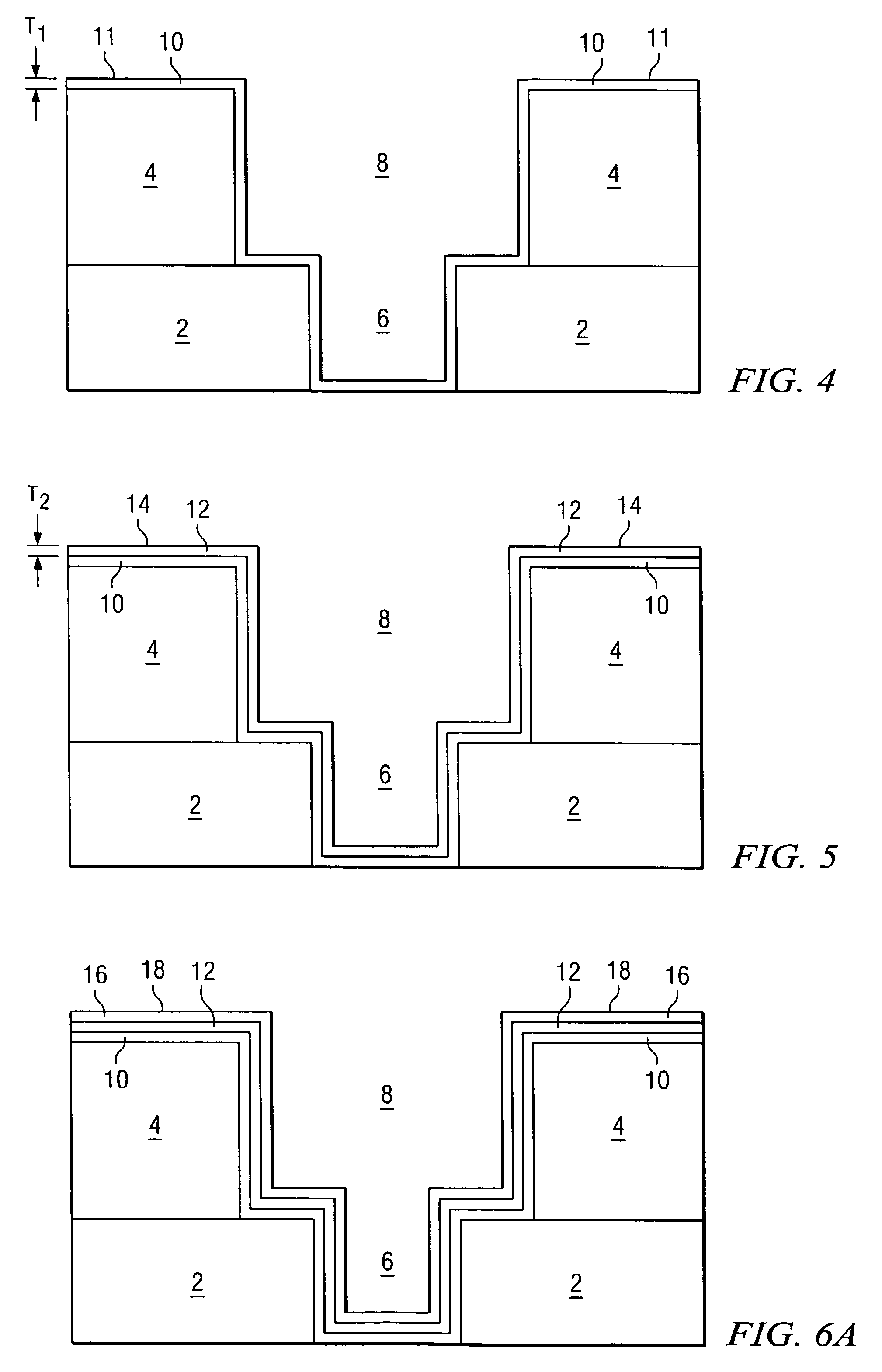
[0017]Damascene interconnect structures typically use copper for its good conductance. When the dimensions of interconnect structures are scaled down to nano-meter range, surface scattering, which indicates how electrons are reflected on the surface (interface) of copper features, begins to play a more significant role. Research has been performed to evaluate the effect of surface scattering. FIG. 1 illustrates a layered structure comprising a dielectric layer 102, a tantalum layer 104 and a copper layer 106. Table 1 lists three samples having a different roughness at the int...


PUM

PropertyMeasurementUnit
dielectric constantaaaaaaaaaa
roughnessaaaaaaaaaa
pressureaaaaaaaaaa

Abstract

An integrated circuit structure having improved resistivity and a method for forming the same are provided. The integrated circuit structure includes a dielectric layer, an opening in the dielectric layer, and a damascene structure in the opening. The damascene structure includes a metallic barrier layer in the opening and in physical contact with the dielectric layer, a conductive material filling the remaining part of the opening, and an interlayer between and adjoining the metallic barrier layer and the conductive material. The interlayer is preferably a metal compound layer.

Description

CROSS-REFERENCE TO RELATED APPLICATION[0001]This application relates to the following commonly assigned, co-pending U.S. patent application: patent application Ser. No. 11 / 429,879, filed on May 8, 2006, and entitled “Reducing Resistivity in Interconnect Structures of Integrated Circuits,” which application is incorporated herein by reference.TECHNICAL FIELD[0002]This invention relates generally to integrated circuits, and more particularly to the structure and formation methods of interconnect structures of integrated circuits.BACKGROUND[0003]In the manufacture of integrated circuits, after individual devices such as transistors have been fabricated on the semiconductor substrate, they must be interconnected in order to perform the desired circuit functions. This interconnection process is generally called “metallization” and is performed using a number of different photolithographic, deposition, and removal techniques.[0004]A commonly used process for forming interconnect structure...

Claims


Application Information

Patent Timeline
Patent Type & Authority Patents(United States)
IPC IPC(8): H01L23/48H01L23/52H01L29/40
CPCH01L21/76807H01L21/76831H01L21/76843H01L21/76844H01L21/76855H01L21/76856H01L23/53238H01L21/76835H01L2924/0002H01L2924/00
Inventor SHIH, CHIH-CHAOHUANG, CHENG-LINHSIEH, CHING-HUASHUE, SHAU-LIN
Owner TAIWAN SEMICON MFG CO LTD
Why Eureka
Try Eureka