Bipolar Junction Transistor Based on CMOS Technology

a bipolar junction transistor and cmos technology, applied in the field of semiconductor technologies, can solve problems such as reducing base resistance, and achieve the effects of high resistivity, high base resistance, and high resistan

Inactive Publication Date: 2012-02-09
DONGBU HITEK CO LTD
View PDF5 Cites 87 Cited by
  • Summary
  • Abstract
  • Description
  • Claims
  • Application Information

AI Technical Summary

Benefits of technology

[0038]Therefore, when incorporating a BJT structure in a CMOS process, a scheme is required in which the current gain β (the ratio of the collector current to the base current) is increased without a change in the profiles of the base and emitter that are provided by CMOS technology.
[0039]An additional drawback of the related art bipolar structure is a high base resistance. A high base resistance results from the fact that the hole current supplied at the base contact flows through a portion of the substrate under the shallow-trench isolation where the resistivity is high and the well layer thickness is reduced. This results in a high voltage drop in the extrinsic base and an increase in noise. This also increases the forward voltage VBE required for a given base current. Therefore, there is a need for a scheme that reduces the base resistance of the BJT.

Problems solved by technology

Additionally, a shallow trench isolation STI between the emitter and the base is absent from the BJT, resulting in reduced base-resistance.

Method used


Image

  • Bipolar Junction Transistor Based on CMOS Technology
  • Bipolar Junction Transistor Based on CMOS Technology
  • Bipolar Junction Transistor Based on CMOS Technology

Examples


Embodiment Construction

[0050]Reference will now be made in detail to the specific embodiments of the present invention, examples of which are illustrated in the accompanying drawings. Wherever possible, the same reference numbers will be used throughout the drawings to refer to the same or like parts.

[0051]A BJT for a CMOS base technology in accordance with a preferred embodiment of the present invention will be described in detail with reference to the attached drawings.

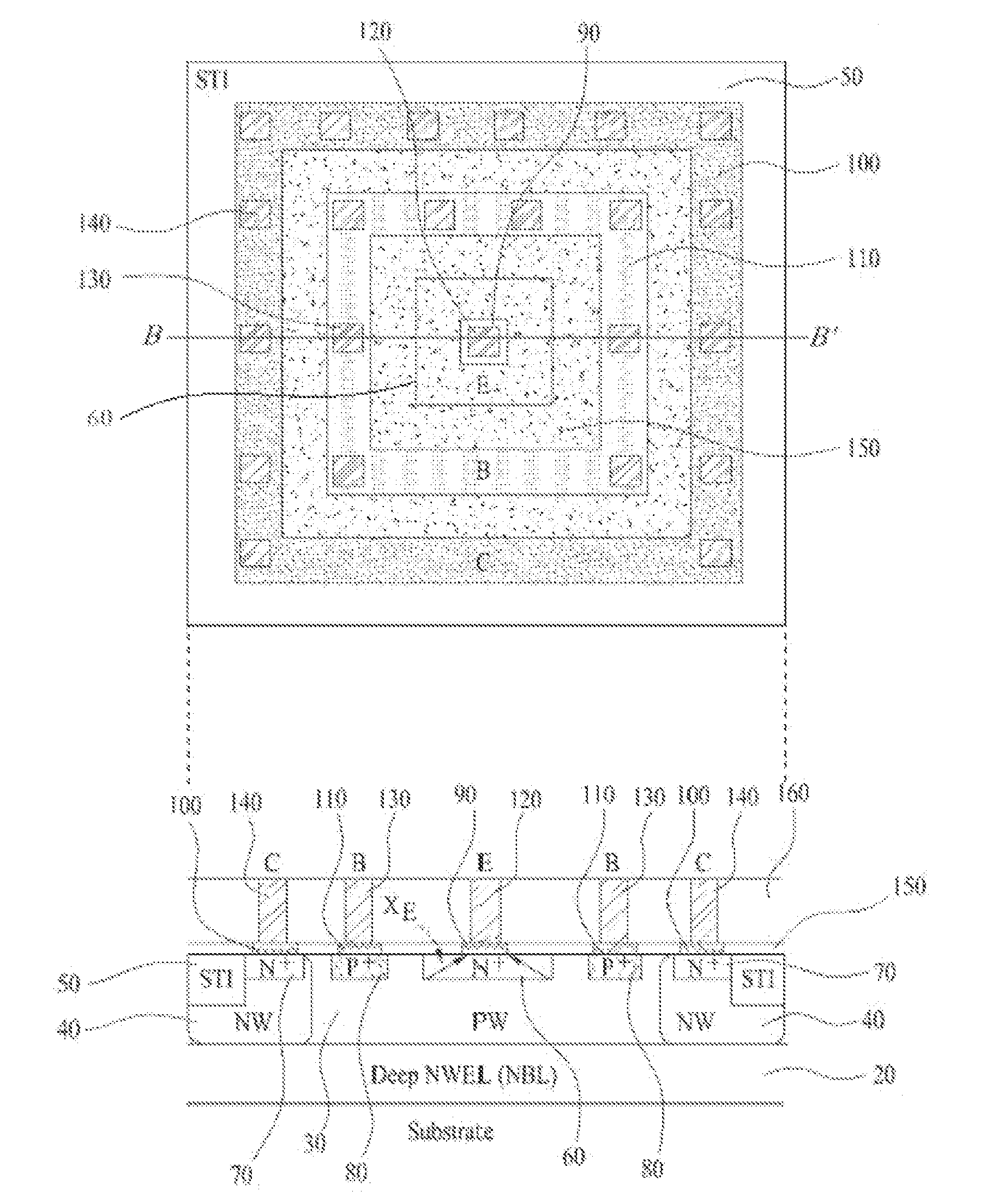
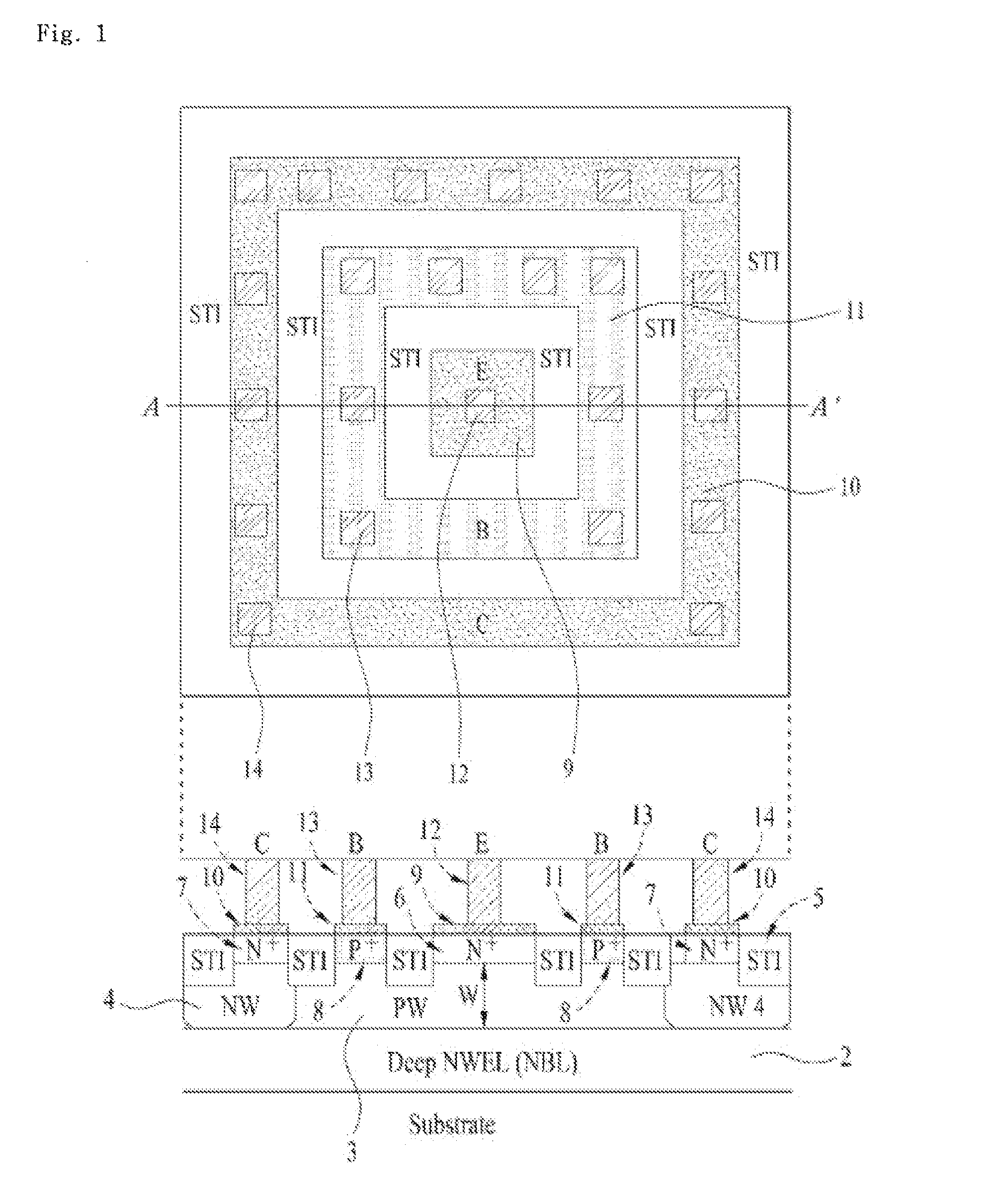
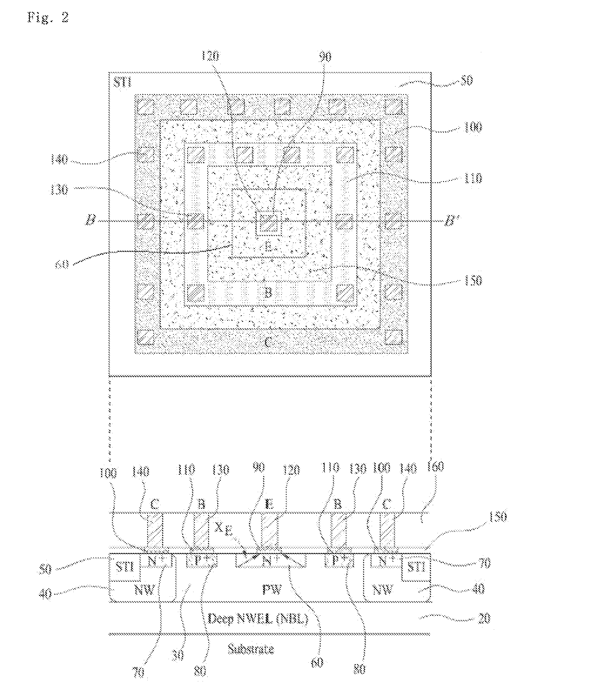
[0052]FIG. 2 illustrates a schematic plan view of a bipolar structure used in a CMOS technology in accordance with a preferred embodiment of the present invention, and a cross section thereof across a line B-B′ shown in the schematic plan view.

[0053]Referring to FIG. 2, there is a plurality of doping regions provided in an active region for forming an emitter, a base, and a collector therein. The structure shown in FIG. 2 illustrates an NPN BJT transistor fabricated on a p-type wafer. A PNP structure similar to that shown in FIG. 2 can be...


PUM


Abstract

The present invention relates to semiconductor technologies, and more particularly to a bipolar junction transistor (BJT) in a CMOS base technology and methods of forming the same. The BJT includes a semiconductor substrate having an emitter region, a base having a first contact, and a collector having a second contact and a well plug; a first silicide film on the first contact; a second silicide film on the second contact; a first silicide blocking layer on or over the semiconductor substrate between the first and second silicide films, and a second silicide blocking layer on the semiconductor substrate between the first silicide film and the emitter region.

Description

CROSS REFERENCE TO RELATED APPLICATION[0001]This application claims the benefit of Korean Patent Application No. 10-2010-0075624, filed on Aug. 5, 2010, which is hereby incorporated by reference as if fully set forth herein.BACKGROUND OF THE DISCLOSURE[0002]1. Field of the Disclosure[0003]The present invention relates to semiconductor technologies, and more particularly to a bipolar junction transistor (BJT) based on a CMOS technology.[0004]2. Discussion of the Related Art[0005]The CMOS technology has been developed toward a high degree of integration, a high operation performance, and low production costs, enabling the use of CMOS devices in many circuit applications, particularly high frequency circuits.[0006]In the meantime, though the CMOS device has excellent operation characteristics, CMOS devices may not adequately meet characteristics required for certain devices in high frequency circuits, such as a low noise amplifiers (LNA), a voltage control oscillators (VCO), and the li...

Claims


Application Information

Patent Timeline
Patent Type & Authority Applications(United States)
IPC IPC(8): H01L29/73H01L21/331
CPCH01L29/0692H01L29/0821H01L29/7322H01L29/66272H01L29/41708
Inventor ELKAREH, BADIHLEE, KYU OKLEE, SANG YONG
Owner DONGBU HITEK CO LTD
Why Eureka
Try Eureka