Display element, optical device, and optical device manufacturing method

a technology of optical devices and display elements, applied in the direction of discharge tubes/lamp details, discharge tubes luminescnet screens, instruments, etc., can solve the problems of difficult to maintain sufficient performance for a long period of time, and in practice it is difficult to obtain a perfectly defect-free film, and achieve excellent sealing characteristics and good display performance.

Active Publication Date: 2009-11-03
JAPAN DISPLAY CENTRAL CO LTD
View PDF13 Cites 21 Cited by
  • Summary
  • Abstract
  • Description
  • Claims
  • Application Information

AI Technical Summary

Benefits of technology

[0009]The present invention has been made in consideration of the above problem, and has as its object to provide a display element which has excellent sealing characteristics and can maintain good display performance, an optical device, and an optical device manufacturing method.

Problems solved by technology

It is difficult in practice to obtain a perfectly defect-free film.
For this reason, each organic EL element cannot be completely shielded from the open air, and it is difficult to maintain sufficient performance for a long period of time.

Method used


Image

  • Display element, optical device, and optical device manufacturing method
  • Display element, optical device, and optical device manufacturing method
  • Display element, optical device, and optical device manufacturing method

Examples


first embodiment

[0075]The first embodiment will exemplify a manufacturing method of cutting array substrates corresponding to a plurality of display devices from one mother substrate. Assume that the mother substrate has a plurality of (e.g., four) array portions to be cut as array substrates.

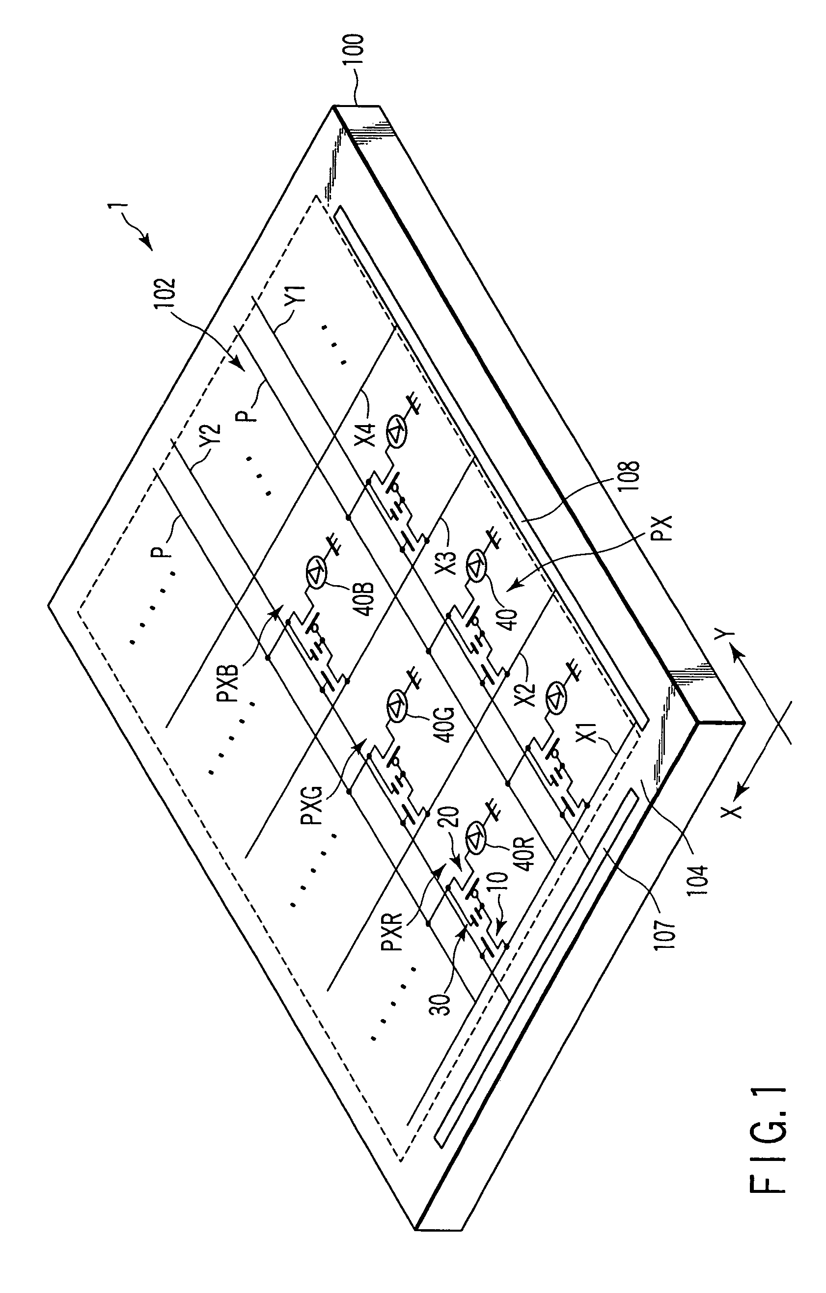
[0076]As shown in FIG. 4A, an effective portion 106 is formed on the major surface of a mother substrate 500. In the first embodiment, four almost rectangular effective portions 106 are formed in correspondence with four array portions AR. Assume that in each array portion AR on the mother substrate 500, each effective portion 106 includes various interconnections such as signal lines Xn, scanning lines Ym, and power supply lines P and a plurality of pixels PX each including an organic EL element 40, in addition to pixel switches 10, drive transistors 20, storage capacitor elements 30, a scanning line driving circuit 107, and a signal line driving circuit 108, which are formed by repeatedly performing processe...

second embodiment

[0112]The second embodiment will exemplify a manufacturing method of cutting array substrates corresponding to a plurality of display devices from one mother substrate. Assume that the mother substrate has a plurality of (e.g., four) array portions to be cut as array substrates.

[0113]As shown in FIG. 8A, effective portions 106 are formed on the major surface of a mother substrate 500. In the second embodiment, as in the first embodiment, four almost rectangular effective portions 106 are formed in correspondence with four array portions AR. In the process of forming the effective portions 106, a plurality of alignment marks AM which are used for the subsequent formation of buffer layers are simultaneously formed. In the second embodiment, in order to stack four buffer layers on each other, four alignment marks AM required to form the respective buffer layers are formed.

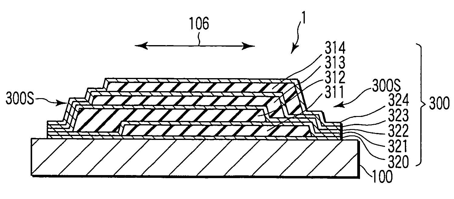
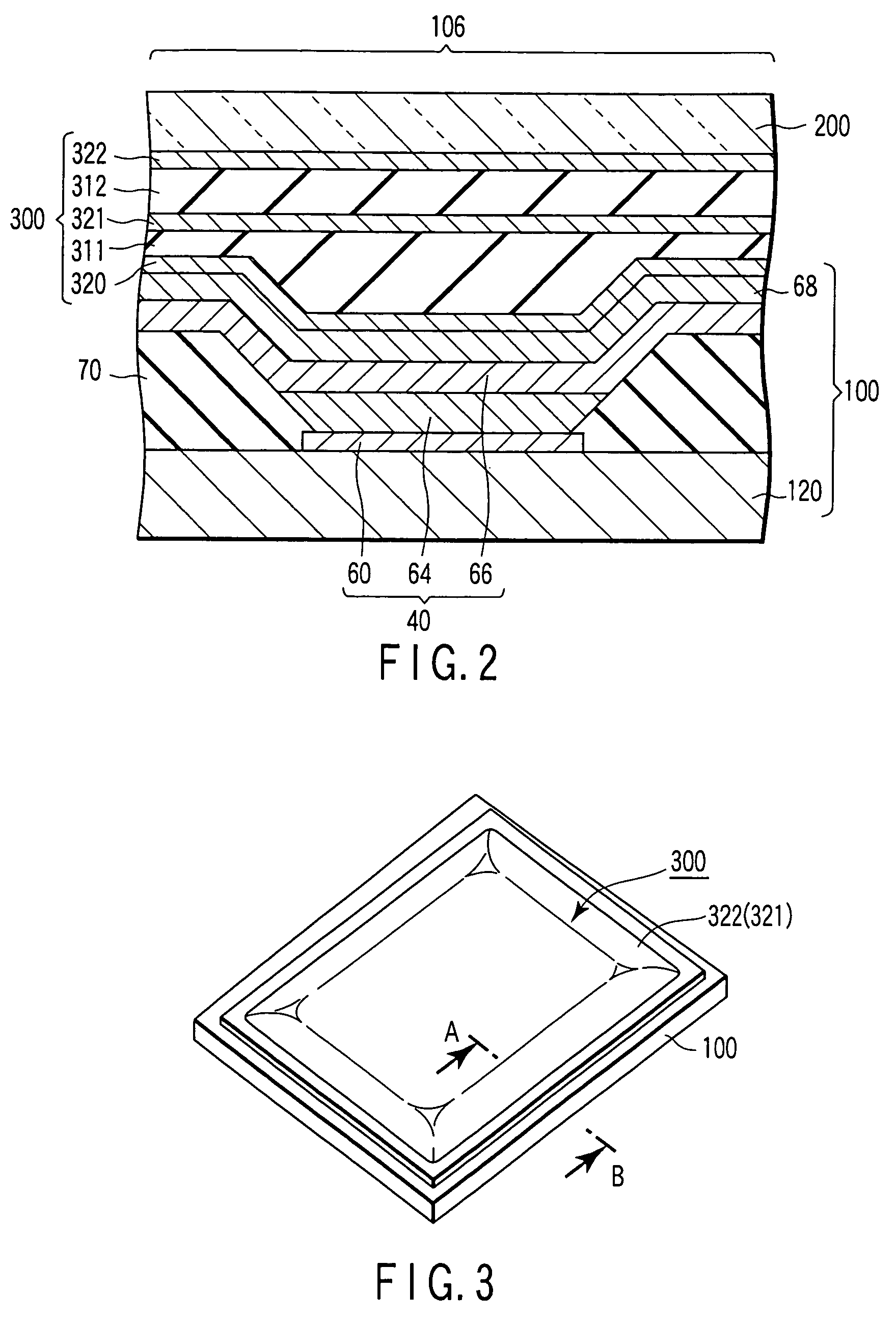
[0114]A sealer 300 is placed to cover at least each effective portion 106 on the major surface of the mother substr...

third embodiment

[0135]The third embodiment will exemplify a case wherein an array substrate corresponding to one display device is manufactured from one substrate. Obviously, both the method of stacking buffer layers on each other while displacing them in one direction as in the first embodiment and the method of stacking buffer layers on each other while displacing them in the four directions as in the second embodiment can be applied to the case wherein one array substrate is manufactured from one substrate as in the third embodiment.

[0136]As shown in FIG. 9A, an array substrate 100 including an effective portion 106 is formed on the major surface of a substrate. In the process of forming the effective portion 106, a plurality of alignment marks AM used for the subsequent formation of buffer layers are simultaneously formed. In the third embodiment, since three buffer layers are stacked, three alignment marks AM required for the formation of the respective buffer layers are formed.

[0137]A sealer ...


PUM

PropertyMeasurementUnit
thicknessaaaaaaaaaa
thicknessaaaaaaaaaa
thicknessesaaaaaaaaaa

Abstract

An array substrate includes an almost rectangular effective portion which is formed on the major surface of the substrate and includes a plurality of pixels for displaying images. An organic EL display device includes a sealer which is placed to cover at least the effective portion on the major surface of the array substrate. The sealer has a structure in which at least two almost rectangular buffer layers which have substantially the same pattern and barrier layers each of which is a pattern larger than each buffer layer and covers each buffer layer to shield it from the open air are stacked on each other. The shortest distance from one side of an end of the effective portion to one side of an end of the first buffer layer is different from the shortest distance to one side of an end of the second buffer layer.

Description

CROSS-REFERENCE TO RELATED APPLICATIONS[0001]This application is based upon and claims the benefit of priority from prior Japanese Patent Applications No. 2003-398084, filed Nov. 27, 2003; and No. 2004-172450, filed Jun. 10, 2004, the entire contents of both of which are incorporated herein by reference.BACKGROUND OF THE INVENTION[0002]1. Field of the Invention[0003]The present invention relates to a display elements an optical device, and an optical device manufacturing method and, more particularly, to an optical device including a plurality of display elements such as self-luminous elements and a method of manufacturing the same.[0004]2. Description of the Related Art[0005]An organic electroluminescence (EL) display device has recently attracted attention as a flat display device. This organic EL display device is a display device including self-luminous elements, and hence has a wide viewing angle and requires no backlight. This makes it possible to realize a flat display device...

Claims


Application Information

Patent Timeline
Patent Type & Authority Patents(United States)
IPC IPC(8): H01J1/62H05B33/00H01L35/24H05B33/04G02F1/13H01J63/04H01L51/52H05B33/02H05B33/10H05B33/12
CPCH01L51/5237H10K50/8426H10K50/846H10K50/8445H10K50/844H05B33/04H05B33/10G02F1/13
Inventor SANO, HIROSHISUMITA, SHIROUYOSHIOKA, TATSUO
Owner JAPAN DISPLAY CENTRAL CO LTD
Why Eureka
Try Eureka