

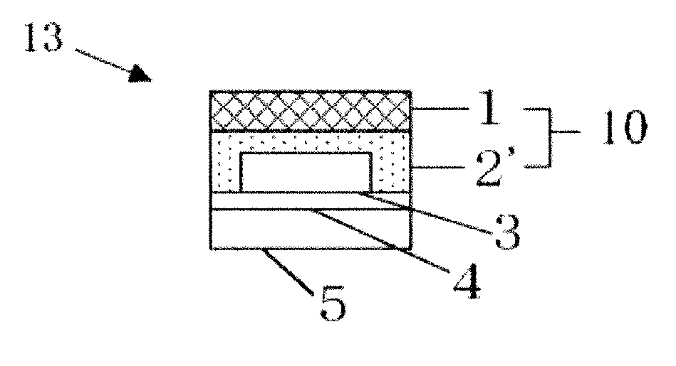
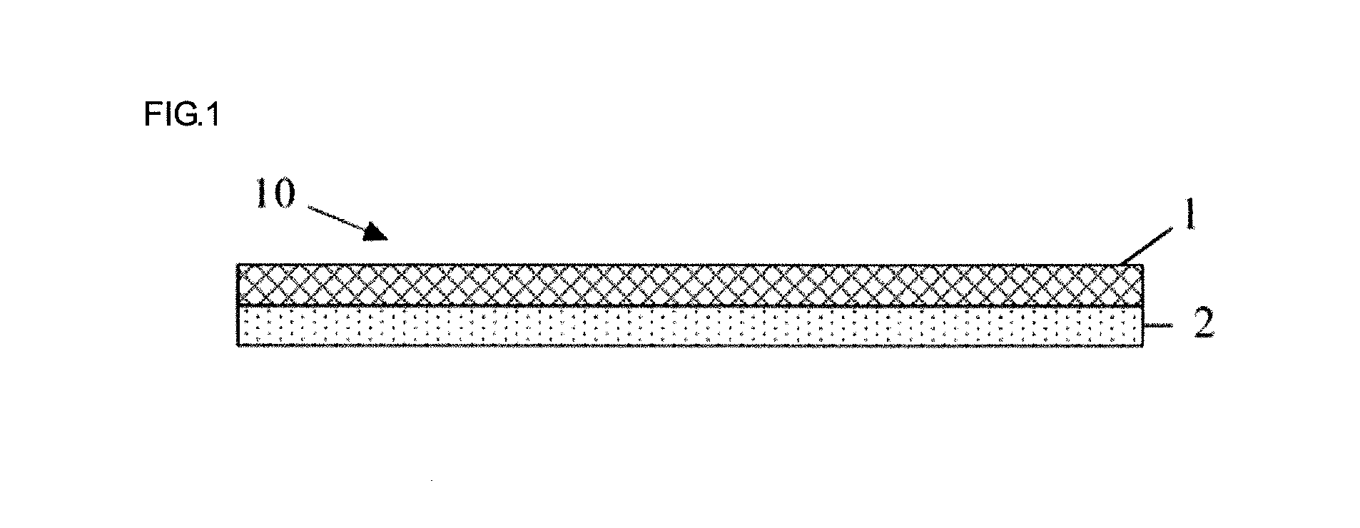
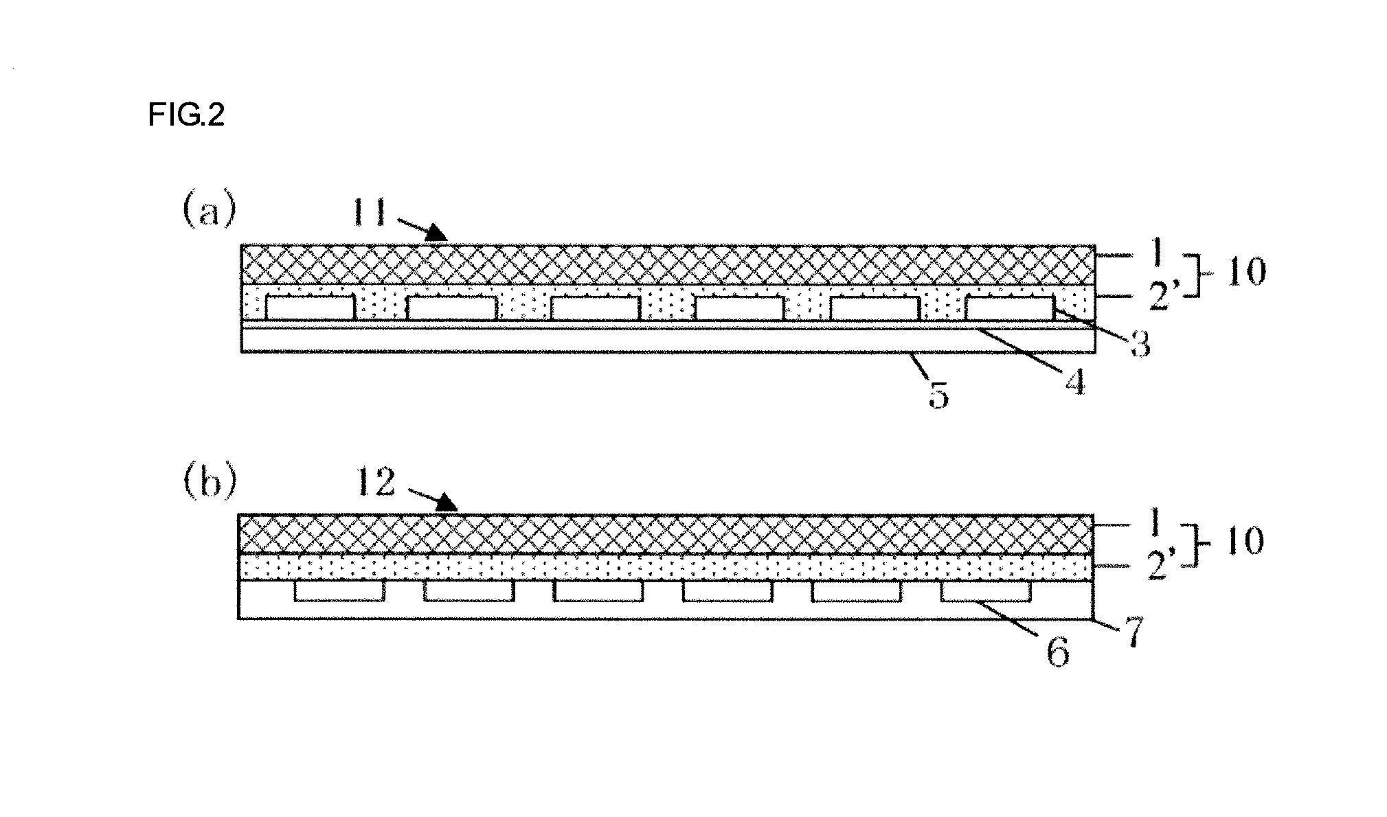
Sealant laminated composite, sealed semiconductor devices mounting substrate, sealed semiconductor devices forming wafer, semiconductor apparatus, and method for manufacturing semiconductor apparatus
- Summary
- Abstract
- Description
- Claims
- Application Information
AI Technical Summary
Benefits of technology
Problems solved by technology
Method used
Image

Examples
synthesis example 1
Organosilicon Compound Having Non-Conjugated Double Bond (A1)
[0126]To synthesize an organosilicon compound having a non-conjugated double bond (A1), 27 mol of organosilane represented as PhSiCl3, 1 mol of ClMe2SiO(Me2SiO)33SiMe2Cl, and 3 mol of MeViSiCl2 were dissolved in a toluene solvent, dropped into wafer, co-hydrolyzed, rinsed, neutralized by alkali cleaning, and dehydrated, and then the solvent was stripped. A composition ratio of constituent units of this compound is represented by an expression: [PhSiO3 / 2]0.27[—SiMe2o-(Me2SiO)33—SiMe2O-]0.01[MeViSiO2 / 2]0.03. A weight-average molecular weight of this compound was 62,000, and a melting point thereof was 60° C. It is to be noted that Vi in the composition formula represents a vinyl group represented by (—CH═CH2), and Me, Ph respectively represent a methyl group and a phenyl group (hereinafter, the same as the above).
Synthesis of Organohydrorgenpolysiloxane
synthesis example 2
Organohydrogenpolysiloxane (B1)
[0127]To synthesize an organohydrorgenpolysiloxane (B1), 27 mol of organosilane represented as PhSiCl3, 1 mol of ClMe2SiO(Me2SiO)33SiMe2Cl, and 3 mol of MeHSiCl2 were dissolved in a toluene solvent, dropped into wafer, co-hydrolyzed, rinsed, neutralized by alkali cleaning, and dehydrated, and then the solvent was stripped. A composition ratio of constituent units of this resin is represented by an expression: [PhSiO3 / 2]0.27[—SiMe2O-(Me2SiO)33—SiMe2O-]0.01[MeHSiO2 / 2]0.03. A weight-average molecular weight of this compound was 58,000, and a melting point of the same was 58° C.
example 1
Fabrication of Composition for Forming Uncured Resin Layer Constituted of Uncured Thermosetting Resin
[0128]With respect to a composition in which 50 parts by mass of the organosilicon compound having a non-conjugated double bond (A1), 50 parts by mass of organohydrogenpolysiloxane (B1), 0.2 parts by mass of acetylene alcohol-based ethynylcyclohexanol as a reaction inhibitor, and 0.1 parts by mass of an octyl alcohol-modified solution of a chloroplatinic acid were added, 350 parts by mass of spherical silica having an average particle size of 5 μm were added at 60° C. and well agitated by a planetary mixer heated to 60° C. to fabricate a silicone resin composition (I-a). The composition was solid at room temperature (25° C.).
Fabrication of Sealant Laminated Composite
[0129]The silicone resin composition (I-a) was sandwiched between a silicon wafer (support wafer) having a diameter of 300 mm (12 inches) and a fluororesin-coated PET film (release film) and compression molded for 5 min u...
PUM
| Property | Measurement | Unit |
|---|---|---|
| Temperature | aaaaa | aaaaa |
| Temperature | aaaaa | aaaaa |
| Fraction | aaaaa | aaaaa |
Abstract
Description
Claims
Application Information