Micro resonator sensor

a micro-resonator and sensor technology, applied in the field of micro-resonator sensors, can solve the problems of etching through intrinsic materials, affecting the accuracy of measurement results, and limiting the aspect of miniaturizing the sensor, so as to minimize radiation loss

Inactive Publication Date: 2009-11-03
CHUNG ANG UNIV IND ACADEMIC COOP FOUND
View PDF10 Cites 19 Cited by
  • Summary
  • Abstract
  • Description
  • Claims
  • Application Information

AI Technical Summary

Benefits of technology

[0027]It is an object of the invention to provide a high-sensitive super-micro resonator sensor, which is integrated as an on-chip to be used whenever and wherever, while minimizing radiation loss incurred by miniaturization of the sensor.

Problems solved by technology

However, although the ring resonator sensor is advantageous in that a characteristic of a measured-material can be measured with a simple configuration, there is a certain limit in the aspect of miniaturizing the sensor.
If the neighborhood of the optical waveguide configuring the ring resonator is deeply etched, although the effect of optical confinement on the side surface of the optical waveguide can be enhanced, there is a problem in that the optical propagation loss is increased due to sidewall roughness.
In addition, if the optical waveguide forming the ring resonator is made of an intrinsic material, etching through the intrinsic material brings about a problem appeared due to excessive surface recombination.
Furthermore, such a ring resonator invites increase of radiation loss and acts as an obstacle to miniaturization of the ring resonator sensor as a result.

Method used


Image

  • Micro resonator sensor
  • Micro resonator sensor
  • Micro resonator sensor

Examples


first embodiment

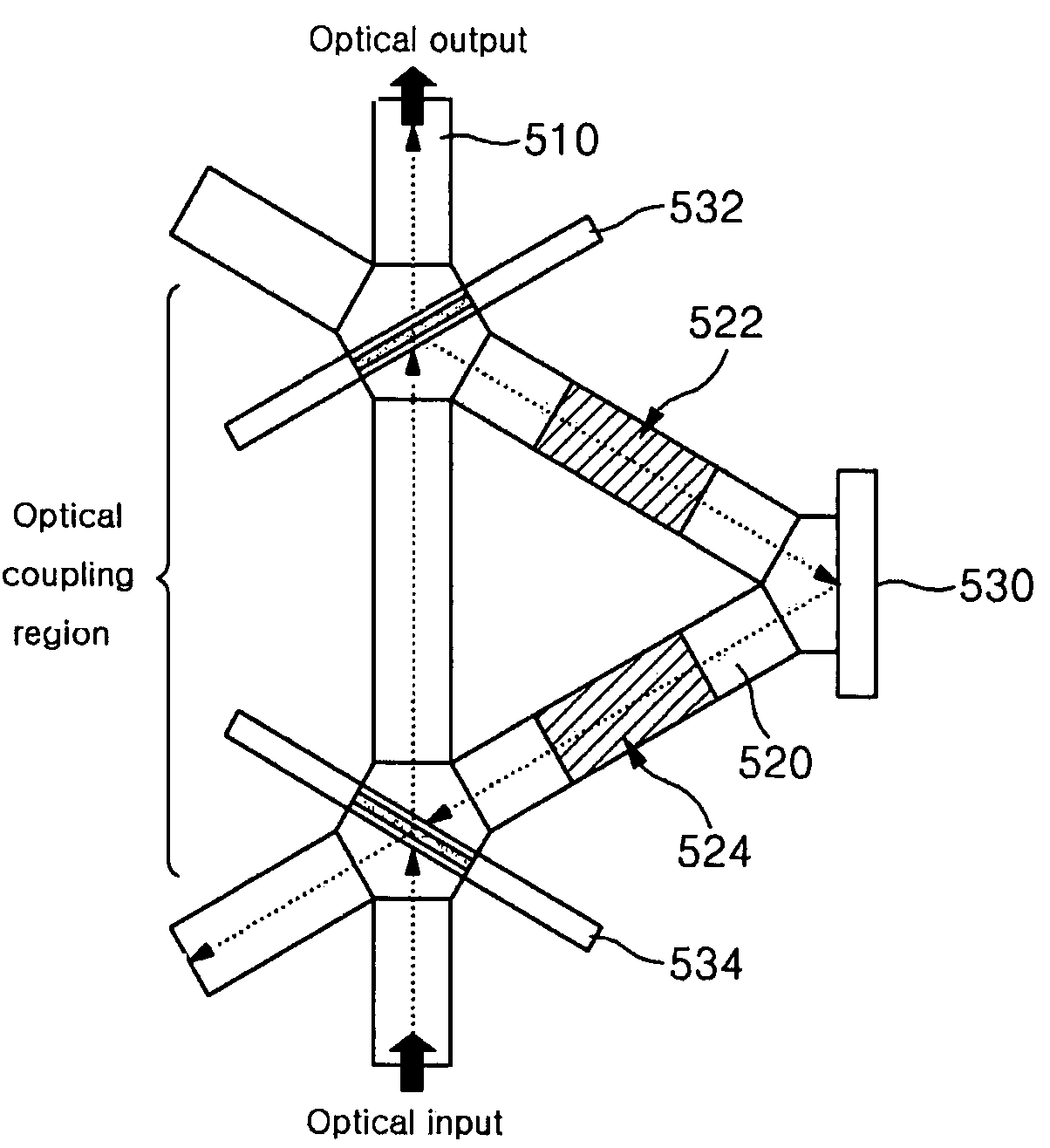
[0050]FIG. 5 is a view showing the configuration of a micro resonator sensor according to the invention.

[0051]Referring to FIG. 5, the micro resonator sensor according to a first embodiment of the invention comprises a main waveguide 510, a resonance waveguide 520, a total reflection mirror 530, and beam splitters 532 and 534. The main waveguide 510 has an incident hole for receiving an optical signal and an exit hole for outputting an optical signal, and an optical coupling region where an optical signal inputted through the incident hole is coupled to the resonance waveguide 520 is formed at the main waveguide 510. The resonance waveguide 520 has an optical coupling region optically connected to the optical coupling region of the main waveguide 510, for receiving an optical signal coupled to the resonance waveguide 520 (hereinafter, referred to as a split optical signal) among the optical signal inputted through the incident hole of the main waveguide 510 in which a plurality of o...

second embodiment

[0054]FIG. 6 is a view showing the configuration of a micro resonator sensor according to the invention.

[0055]Referring to FIG. 6, the micro resonator sensor according to a second embodiment of the invention comprises a main waveguide 540, a resonance waveguide 550, and total reflection mirrors 560, 562, and 564. The main waveguide 540 has an incident hole for receiving an optical signal and an exit hole for outputting an optical signal, and an optical coupling region where the optical signal inputted through the incident hole is coupled to the resonance waveguide 550 is formed at the main waveguide 540. The resonance waveguide 550 has an optical coupling region optically connected to the optical coupling region of the main waveguide 540, for receiving an optical signal coupled to the resonance waveguide 550 among the optical signal inputted through the incident hole of the main waveguide 540, and a plurality of optical waveguides is arranged in a triangular shape. At this point, on...

third embodiment

[0057]FIG. 7 is a view showing the configuration of a micro resonator sensor according to the invention.

[0058]Referring to FIG. 7, the micro resonator sensor according to a third embodiment of the invention comprises a main waveguide 570, an optical coupler 575, a resonance waveguide 580, and total reflection mirrors 590, 592, 594, and 596. The main waveguide 570 has an incident hole for receiving an optical signal and an exit hole for outputting an optical signal, and an optical coupling region where the optical signal inputted through the incident hole is coupled to the optical coupler 575 is formed at the main waveguide 570. The optical coupler 575 splits the optical signal inputted through the incident hole of the main waveguide 570 to the exit hole of the main waveguide 570 and the resonance waveguide 580. In addition, the optical coupler 575 splits the optical signal that has circulated inside the resonance waveguide 580 to the exit hole of the main waveguide 570 and to the re...


PUM


Abstract

A micro resonator sensor includes a main waveguide, a resonance waveguide and optical path changing means. Optical path changing means are installed at apex regions contacting with adjacent optical waveguides forming the resonance waveguide and reflect at least a part of the split optical signal inputted into the resonance waveguide to circulate the split optical signal inside the resonance waveguide. The micro resonator sensor can be manufactured without an excessive radiation loss and can be manufactured as an on-chip.

Description

CROSS-REFERENCE TO RELATED APPLICATIONS[0001]This application claims the benefit of priority of Korean Patent Application No. 10-2006-0108579 filed on Nov. 3, 2006, which are incorporated by reference in their entirety herein.BACKGROUND[0002]1. Technical Field[0003]The present invention relates to a micro resonator sensor, and more specifically, to a sensor for detecting a characteristic of a material to be measured (also called “to-be-measured material”) using changes in a refractive index of a resonator.[0004]2. Related Art[0005]Generally, a resonator sensor serves to detect a characteristic of a measured-material by detecting intensity of light at the output terminal of a waveguide that is formed with an input terminal and an output terminal. In this case, the intensity of light corresponds to a change of an effective refractive index of a ring resonator that occurs when light traveling through the waveguide is coupled to the ring resonator installed to be spaced apart from the w...

Claims


Application Information

Patent Timeline
Patent Type & Authority Patents(United States)
IPC IPC(8): G01C3/14G01B9/02
CPCG01N21/7746G02B6/12007G01N2021/7779G01J1/44
Inventor CHOI, YOUNG-WANKIM, DOO-GUN
Owner CHUNG ANG UNIV IND ACADEMIC COOP FOUND
Why Eureka
Try Eureka