Circuit board via structure and method forming the same

a circuit board and hole technology, applied in the direction of printed circuit manufacturing, printed circuit aspects, printed circuit electric connection formation, etc., can solve the problems of adverse impact on the system using the pcb, affecting signal quality,

Inactive Publication Date: 2011-01-13
YINGHUADA (SHANGHAI) ELECTRONIC CO LTD +1
View PDF36 Cites 6 Cited by
  • Summary
  • Abstract
  • Description
  • Claims
  • Application Information

AI Technical Summary

Problems solved by technology

Specifically, when the PCB 5 includes a radio frequency signal wire and the wire is positioned close to the via hole, since the frequency of radio frequenc...

Method used


Image

  • Circuit board via structure and method forming the same
  • Circuit board via structure and method forming the same
  • Circuit board via structure and method forming the same

Examples


Embodiment Construction

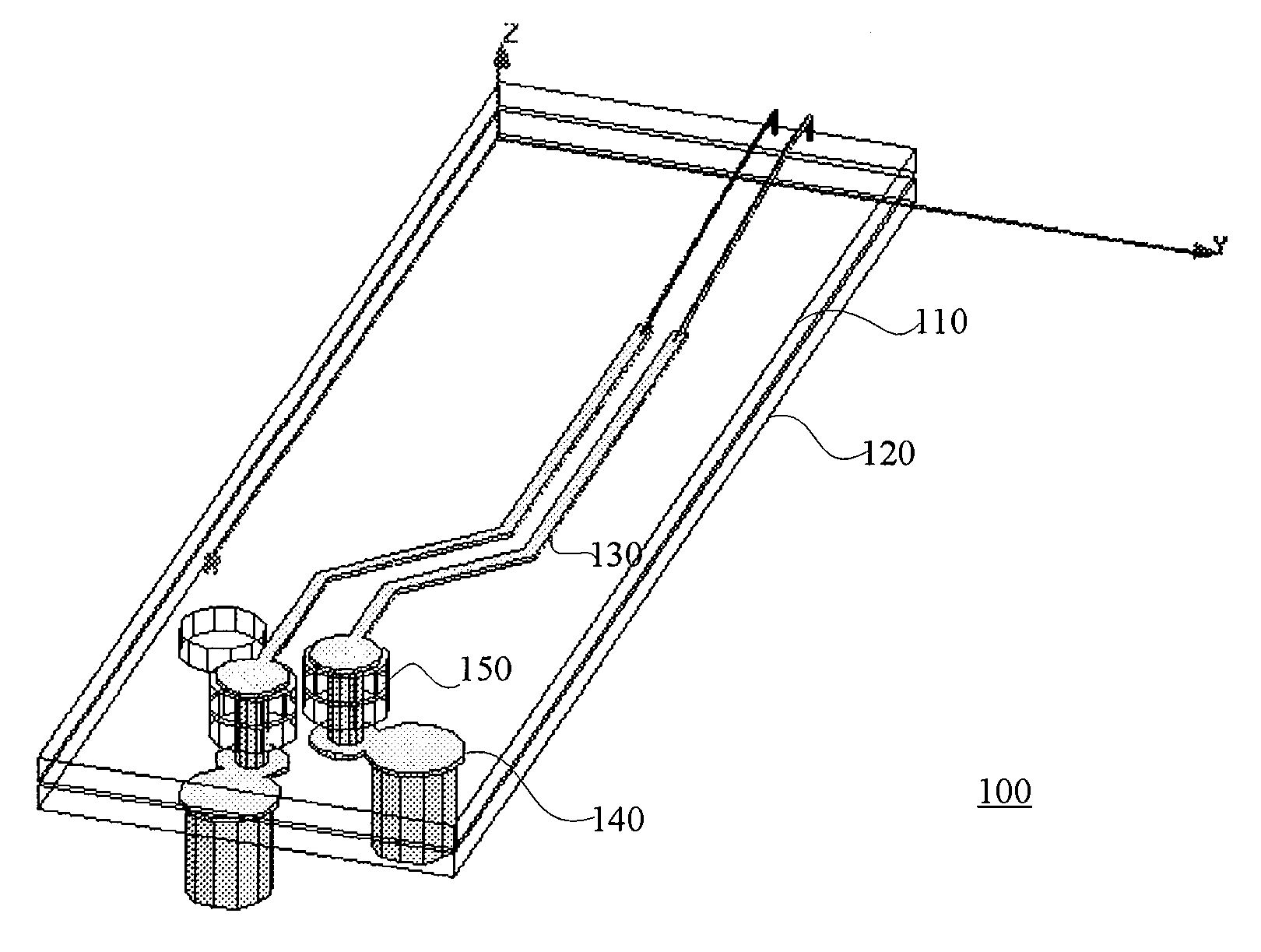
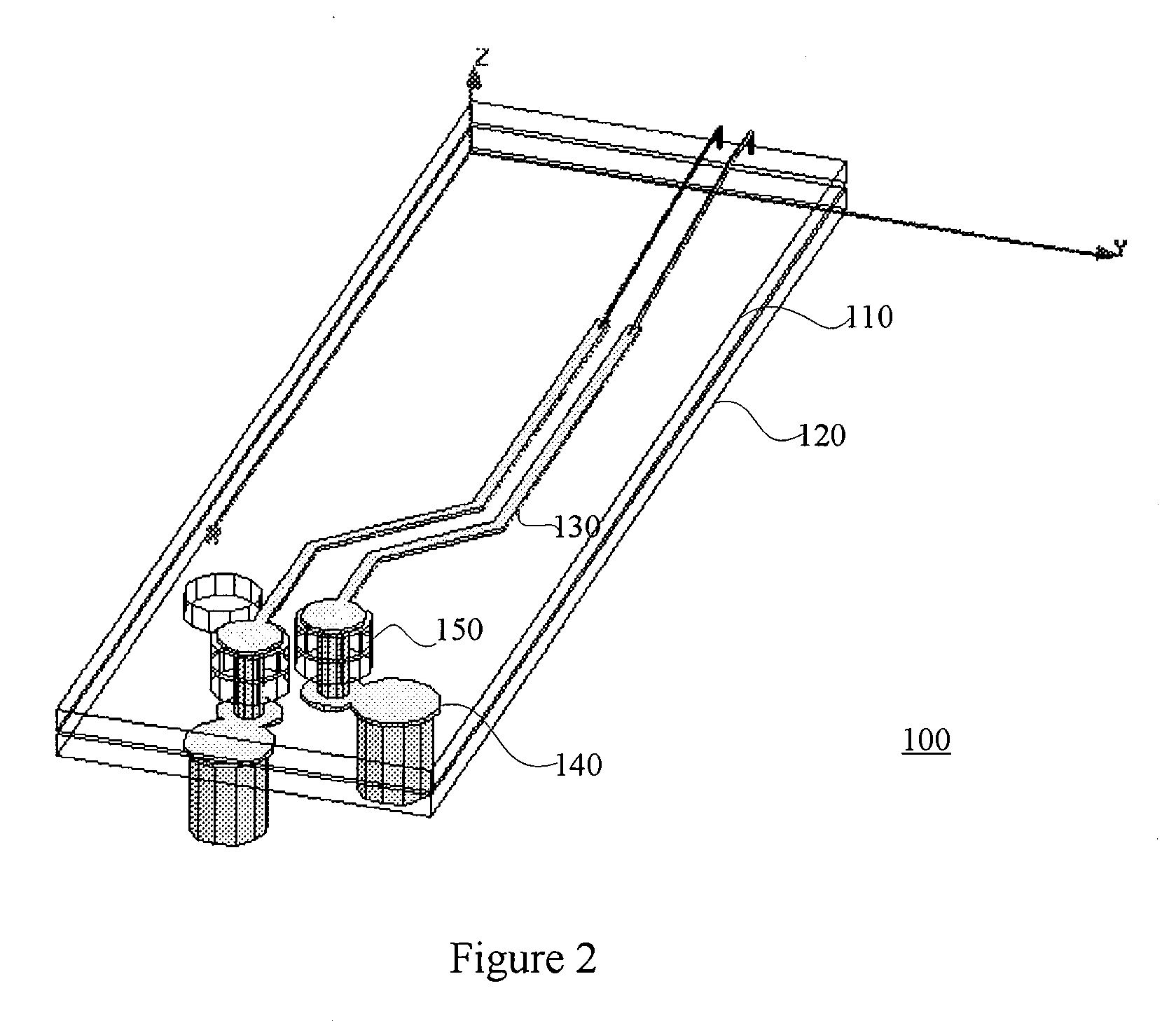
[0011]FIG. 2 is a perspective view of a double layer printed circuit board (“PCB”) 100 according to an embodiment of the present invention. The PCB 100 includes a top routing layer 110 and a bottom routing layer 120. The top routing layer 110 includes a circuit (not shown) having a radio frequency wire 130 arranged thereon, and the bottom routing layer 120 includes at least one electronic component 140 positioned thereon. The PCB 100 also includes a via hole structure 150 formed therein. The via hole structure 150 connects the radio frequency wire 130 with the electronic component 140, thereby facilitating the transmission of radio frequency signals between the wire 130 and the component 140. It is appreciated that the electronic component 140 may be an electrical device connected with the via hole structure 150 or a welding foot (not shown). It is also appreciated that the top routing layer 110 and the bottom routing layer 120 may include a radio frequency circuit as well as any ot...


PUM

PropertyMeasurementUnit
Diameteraaaaaaaaaa
Structureaaaaaaaaaa
Electrical conductoraaaaaaaaaa

Abstract

A printed circuit board (“PCB”) (100) includes a first routing layer (110), a second routing layer (120) and a via hole structure (150) electrically connecting the two routing layers. The via hole structure (150) includes a connecting hole (158) extending between the first routing layer (110) and the second routing layer (120), an inner conductor (154) positioned in the connecting hole (158), an outer conductor (152) substantially surrounds the inner conductor (154), and an insulating medium (156) positioned between the inner conductor and the outer conductor. The outer conductor (152) is insulated from the inner conductor (154), the outer conductor (152) is configured to connected to the ground, and the inner conductor (154) is configured to transmit signals.

Description

FIELD OF INVENTION[0001]The present invention relates to via hole structures between different routing layers and printed circuit boards (“PCBs”) having such via hole structures.BACKGROUND OF INVENTION[0002]With the development of very large scale integrated (VLSI) circuit technologies, printed circuit boards (“PCBs”) have been widely used. Generally, there are three types of PCBs: single layer PCB, double layer PCB and multi-layer PCB.[0003]Generally, a single layer PCB is a circuit board that only has one side clad with copper, and has electronic components placed on the other side. The copper-clad side is for routing and components welding. A double layer PCB is a circuit board that has both sides clad with copper, and the two copper layers are often referred to as the top layer and the bottom layer. Wires can be routed on both copper-clad sides. The top layer is generally for placing components thereon, and the bottom layer is generally for welding the components. The multi laye...

Claims


Application Information

Patent Timeline
IPC IPC(8): H05K1/09H05K1/11C25D5/02H05K3/42H05K3/32
CPCH05K1/0222H05K2201/0949H05K2201/09618Y10T29/49128H05K2201/09718H05K2201/09809Y10T29/49165H05K2201/09645H05K2201/09609
Inventor LIU, PENGZHANG, YUTSAI, SHIH-KUANG
Owner YINGHUADA (SHANGHAI) ELECTRONIC CO LTD
Why Eureka
Try Eureka