Circuit technique to prevent device overstress

a circuit technique and device technology, applied in the field of circuit technique to prevent device overstress, can solve the problems of regulated voltage output of the regulator, inadvertent configuration of the regulator in an unknown and, possibly, less than optimal manner, and failure of the device immediately or prematurely

Active Publication Date: 2009-11-17
NVIDIA CORP
View PDF5 Cites 24 Cited by
  • Summary
  • Abstract
  • Description
  • Claims
  • Application Information

AI Technical Summary

Benefits of technology

[0010]Embodiments of the present invention generally provide methods and apparatus for preventing the application of voltages outside a rated tolerance to circuit components in an integrated circuit device.

Problems solved by technology

Unfortunately, during power up or power down of the device, the I / O supply voltage may reach its final value while the core supply voltage is still ramping up or is completely off.
As a result, the regulator may be inadvertently configured in an unknown and, possibly, less than optimal manner.
This situation may cause the regulated voltages output by the regulator and internal bias levels (inside of regulator) to be much higher than the maximum tolerance levels of these devices.
This type of overstressing may lead to immediate or premature device failure.
However, this approach is also suboptimal as it adds components to the system bill of materials (BOMs) and increases overall cost and complexity.

Method used


Image

  • Circuit technique to prevent device overstress
  • Circuit technique to prevent device overstress
  • Circuit technique to prevent device overstress

Examples


Embodiment Construction

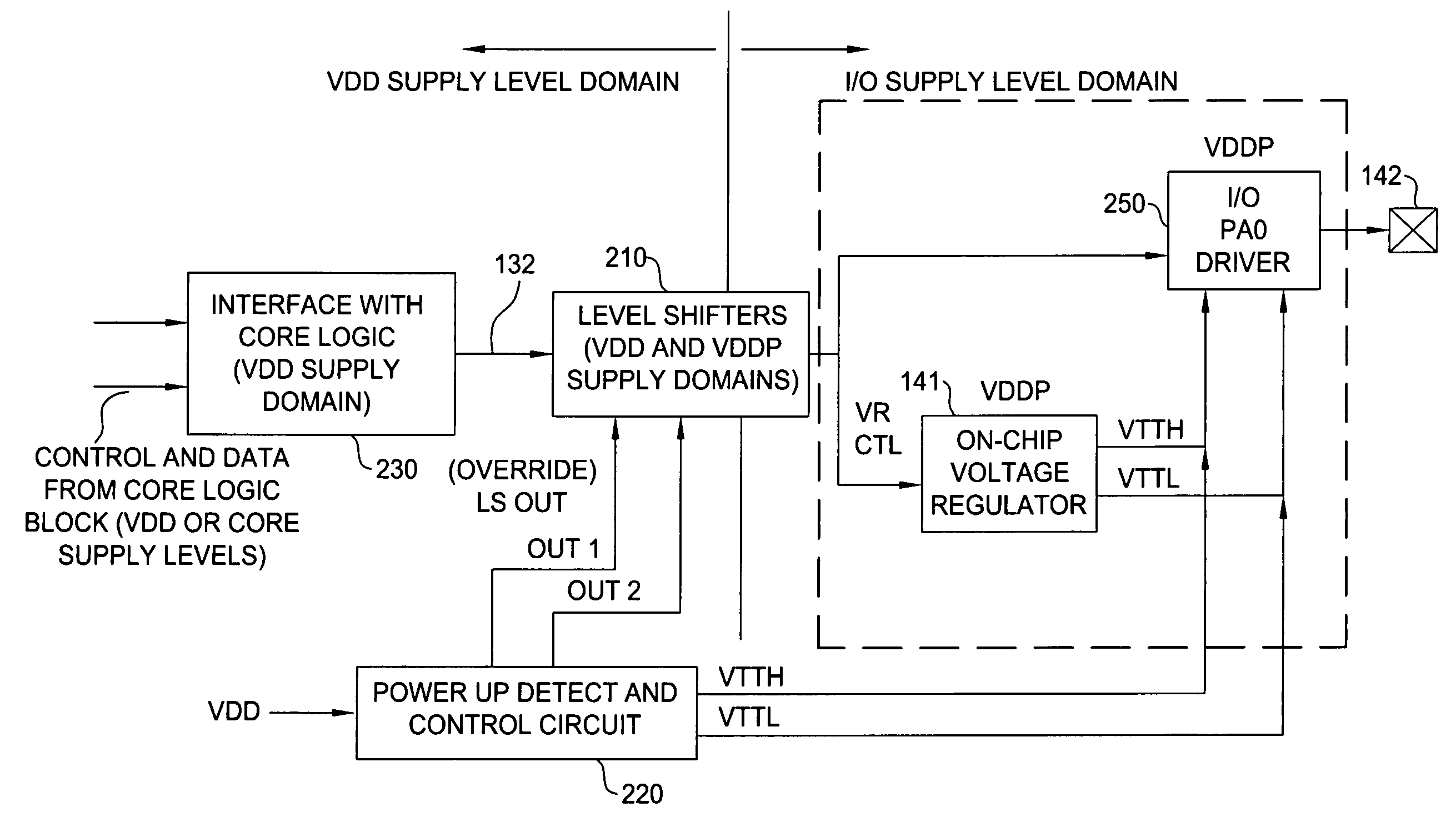
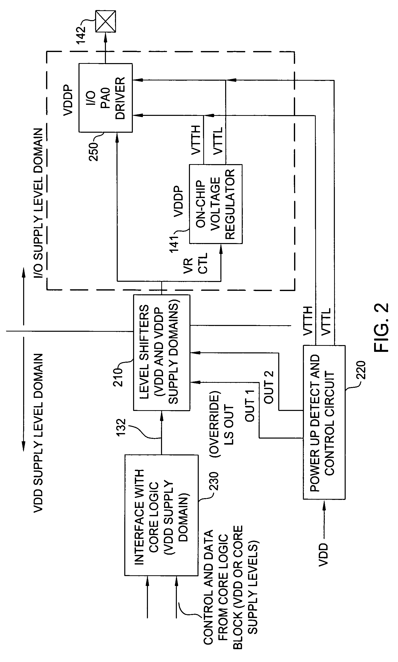
[0023]Embodiments of the present invention provide a technique for ensuring voltage levels outside a rated voltage tolerance are not inadvertently applied to I / O logic circuit components in an integrated circuit device due to core logic and I / O logic supply voltages reaching final voltage levels at different times. According to some embodiments, an internal voltage supply sense circuit may monitor a level of a voltage supply that powers core logic that generates control signals to configure an on-chip voltage regulator used to generate regulated voltages for the I / O logic. The sense circuit may generate one or more voltage bias signals used to keep the regulated voltages supplied to the I / O logic in a defined state even in the absence of core logic supply voltage.

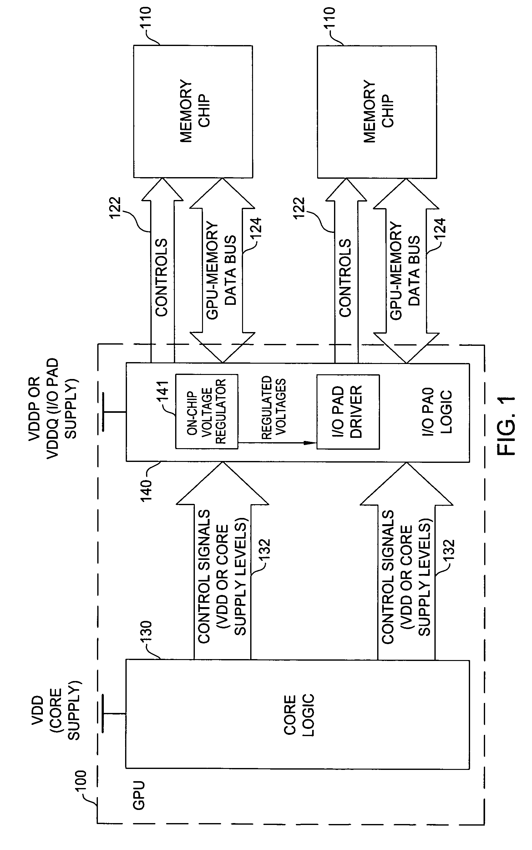
[0024]As a specific, but not limiting example, one embodiment of the present invention provides a graphics processing unit (GPU) with an internal circuit that monitors core logic supply voltage and generates one or more bia...


PUM


Abstract

Techniques and circuits for ensuring one or more circuit components are not subjected to voltage levels above their rated voltage tolerance due to core logic and I/O logic supply voltages reaching final voltage levels at different times are provided. According to some embodiments, an internal voltage supply sense circuit may monitor a level of a voltage supply that powers core logic that generates control signals used to program a voltage regulator. In response to determining the core logic voltage supply is below a predetermined level, the sense circuit may generate one or more regulated voltage signals to override regulated voltage signals generated by the voltage regulator.

Description

CROSS-REFERENCE TO RELATED APPLICATIONS[0001]This application is related to co-pending U.S. patent application Ser. No. 11 / 299,081 entitled, “CIRCUIT TECHNIQUE TO ACHIEVE POWER UP TRISTATE ON A MEMORY BUS”, filed herewith and incorporated herein in its entirety.BACKGROUND OF THE INVENTION[0002]1. Field of the Invention[0003]This invention relates generally to computer systems and more specifically to a technique for ensuring circuit devices are not overstressed by operating voltages above their rated tolerance.[0004]2. Description of the Related Art[0005]In a typical processor device, such as a central processor unit (CPU) or graphics processing unit (GPU), different logic portions may be powered from different supply voltages. For example, in a GPU, core processing logic that processes data and generates command signals to external devices (e.g., memory devices) may be powered from a first supply voltage (e.g., VDD), while input output (I / O) logic that drives those command signals ...

Claims


Application Information

Patent Timeline
Patent Type & Authority Patents(United States)
IPC IPC(8): H03K19/0175H03K19/094
CPCH03K19/017545
Inventor SHAIKH, ASHFAQ R.HONG, CHANG HEEKU, TING-SHENG
Owner NVIDIA CORP
Why Eureka
Try Eureka