Parallel bit test circuit and method for semiconductor memory device

a semiconductor memory and parallel bit test technology, applied in measurement devices, error detection/correction, instruments, etc., can solve the problems of parallel bit test failing to identify the defective memory cells, the failure of parallel bit test to manufacture a semiconductor memory device without any defects at all, and the defective memory cells in the pair

Active Publication Date: 2009-11-24
SAMSUNG ELECTRONICS CO LTD
View PDF18 Cites 5 Cited by
  • Summary
  • Abstract
  • Description
  • Claims
  • Application Information

AI Technical Summary

Benefits of technology

[0013]Embodiments of the invention provide a parallel bit test circuit and associated methods adapted to eliminate a limit in a range of test data patterns that can be used to test a semiconductor memory device for defective cells.

Problems solved by technology

In practice, it is very difficult to manufacture a semiconductor memory device without any defects at all.
Unfortunately, all pairwise bit comparisons in the method illustrated in FIG. 1 take place between bits in the same memory block.
However, defective memory cells in the same memory block may be correlated, and therefore even if the parallel bit test indicates that both memory cells in a pair store the same data, it is likely that both memory cells in a pair are defective and that the parallel bit test will fail to identify those defective memory cells.
As a result, it is difficult for the conventional method parallel bit test method to detect all of the defective memory cells in a semiconductor memory device.

Method used


Image

  • Parallel bit test circuit and method for semiconductor memory device
  • Parallel bit test circuit and method for semiconductor memory device
  • Parallel bit test circuit and method for semiconductor memory device

Examples


Embodiment Construction

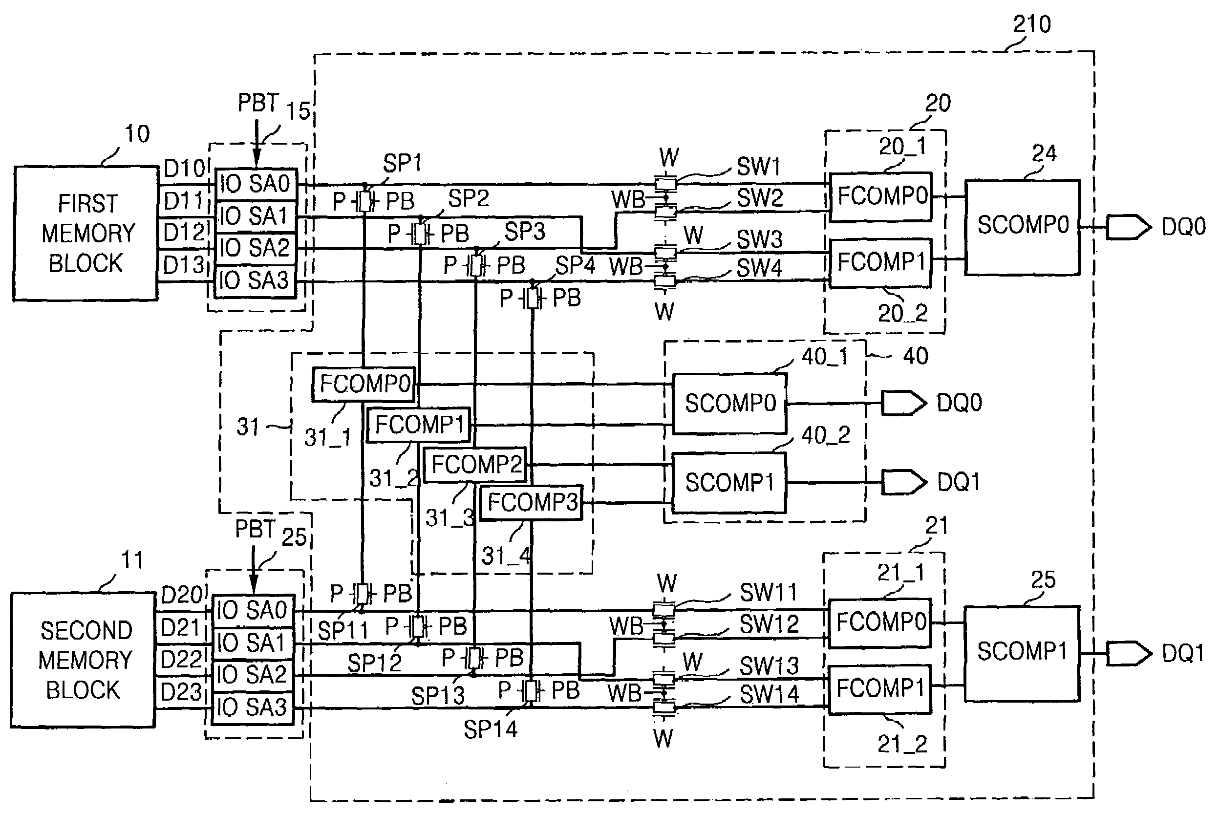
[0023]Exemplary embodiments of the invention are described below with reference to the corresponding drawings. These embodiments are presented as teaching examples. The actual scope of the invention is defined by the claims.

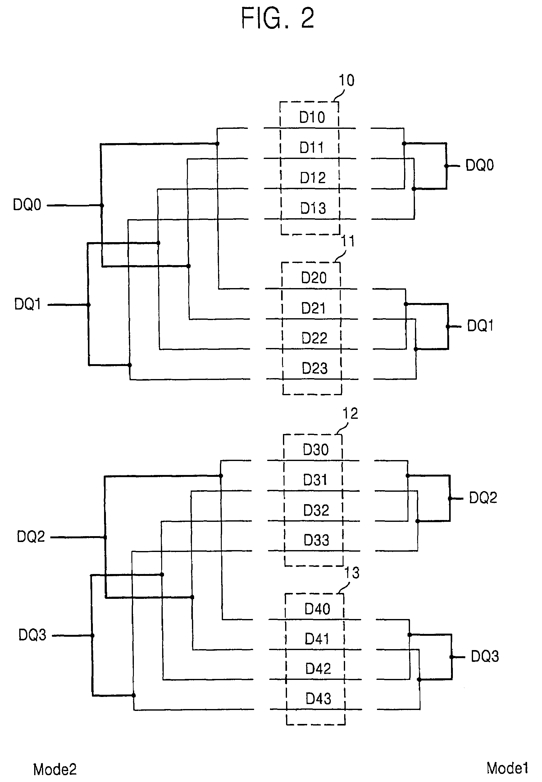
[0024]FIG. 2 is a conceptual diagram illustrating a parallel bit test method for a semiconductor memory device according to an embodiment of the present invention. Referring to FIG. 2, the parallel bit test method can be performed in two different modes, both of which are parallel bit test (PBT) modes. In a first test mode Mode1, also referred to as a wafer test mode, the method is performed in a wafer stage before repairs are performed on the semiconductor memory device. In a second test mode Mode2, also referred to as a package test mode, the method is performed in a package stage after the repairs have been performed on the semiconductor memory device.

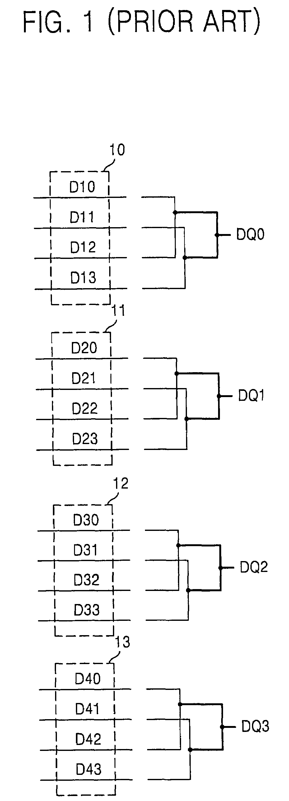
[0025]The parallel bit test method performed in first test mode Mode1 is similar to the conventional parallel ...


PUM


Abstract

A semiconductor memory device performs a parallel bit test on a plurality of memory blocks by writing test pattern data into the plurality of memory blocks, outputting two bits from each memory block in parallel and comparing the two bits output from each memory block with each other in a first test mode, and outputting two bits from respectively different memory blocks and comparing the two bits output from the respectively different memory blocks with each other in a second test mode.

Description

BACKGROUND OF THE INVENTION[0001]1. Field of the Invention[0002]Embodiments of the present invention relate generally to semiconductor memory devices. More particularly, embodiments of the invention relate to parallel bit test (PBT) circuits and methods of testing memory cells in semiconductor memory devices using the PBT circuits.[0003]A claim of priority is made to Korean Patent Application No. 10-2006-51618, filed on Jun. 8, 2006, the disclosure of which is hereby incorporated by reference in its entirety.[0004]2. Description of Related Art[0005]Semiconductor memory devices are typically manufactured by performing several design and processing steps on a semiconductor wafer. Following manufacture, the semiconductor memory devices are then tested for defects. This testing often occurs both after performing the processing steps on the semiconductor wafer and after the semiconductor memory devices are packaged. The testing performed after processing the wafer is commonly referred to...

Claims


Application Information

Patent Timeline
Patent Type & Authority Patents(United States)
IPC IPC(8): G11C29/00
CPCG11C29/40G11C2029/4002G11C29/00
Inventor BYUN, SANG-MANKANG, SANG-SEOK
Owner SAMSUNG ELECTRONICS CO LTD
Why Eureka
Try Eureka