Semiconductor device

a technology of semiconductor devices and semiconductors, applied in semiconductor devices, solid-state devices, instruments, etc., can solve the problems of short data retention period, difficult to sufficiently reduce power consumption, and loss of stored data, so as to reduce power consumption and reduce power consumption. the effect of short channel effect, short channel effect, and increased storage capacity per unit area

Active Publication Date: 2014-08-19
SEMICON ENERGY LAB CO LTD
View PDF128 Cites 45 Cited by
  • Summary
  • Abstract
  • Description
  • Claims
  • Application Information

AI Technical Summary

Benefits of technology

[0013]It is an object of one embodiment of the disclosed invention to provide a highly integrated semiconductor device with a novel structure and to increase storage capacity per unit area.
[0014]It is an object to suppress a short channel effect in a highly integrated semiconductor device with a novel structure.
[0031]In one embodiment of the disclosed invention, a semiconductor device is formed using a material which can sufficiently reduce off-state current of a transistor, for example, an oxide semiconductor material that is a wide-gap semiconductor. With the use of a semiconductor material which can sufficiently reduce off-state current of a transistor, data can be retained for a long time.
[0032]In one embodiment of the disclosed invention, data is written by switching of on and off of a transistor including an oxide semiconductor material. Thus, it is possible to remove limitations on the number of writing because data writing does not need high voltage and elements are not degraded.
[0034]In one embodiment of the disclosed invention, a connection electrode for connecting a transistor including a semiconductor material other than an oxide semiconductor to a transistor including an oxide semiconductor material is made smaller than an electrode of the transistor including a semiconductor material other than an oxide semiconductor that is connected to the connection electrode. Thus, the area of the transistor including an oxide semiconductor material that is connected to the connection electrode can be decreased, so that a semiconductor device with a novel structure can be highly integrated and storage capacity per unit area can be increased.
[0035]In one embodiment of the disclosed invention, an oxide semiconductor layer of a transistor including an oxide semiconductor material is provided to be in contact with a bottom surface and an inner wall surface of a trench formed in an insulating layer. Thus, the channel length of the transistor can be made longer as compared to the case where the oxide semiconductor layer is formed on a plane, so that a short channel effect can be suppressed.

Problems solved by technology

Further, a transistor included in a storage element has leakage current (off-state current) or the like between a source and a drain in an off state and electric charge flows into or out even if the transistor is not selected, so that a data retention period is short.
For that reason, another writing operation (refresh operation) is necessary at predetermined intervals, and it is difficult to sufficiently reduce power consumption.
Furthermore, since stored data is lost when power is not supplied, a different storage device including a magnetic material or an optical material is needed in order to retain data for a long time.
However, cost per storage capacity is high because a circuit such as a flip-flop is used.
Further, as in a DRAM, stored data in an SRAM is lost when power is not supplied.
However, there is a problem in that a storage element does not function after a predetermined number of writing operations because a gate insulating layer included in the storage element is degraded by tunneling current generated in writing operations.
However, this method needs a complex peripheral circuit.
Further, even when such a method is employed, fundamental life problems cannot be solved.
That is, a flash memory is not suitable for applications in which data is frequently rewritten.
Further, it takes a comparatively long time to inject or remove electric charge, and it is not easy to increase the speed of writing or erasing data.

Method used


Image

  • Semiconductor device
  • Semiconductor device
  • Semiconductor device

Examples


embodiment 1

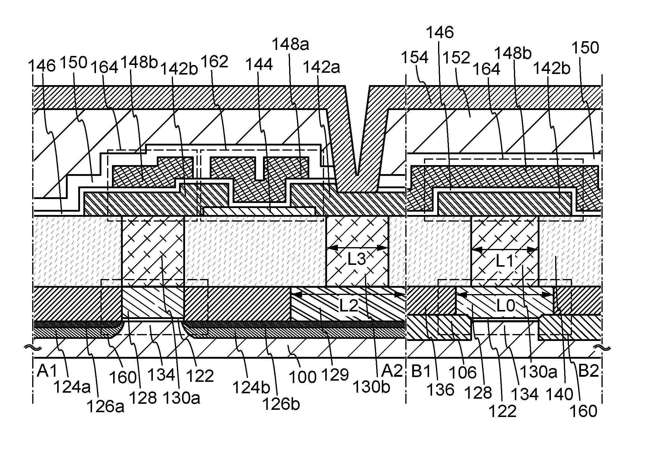
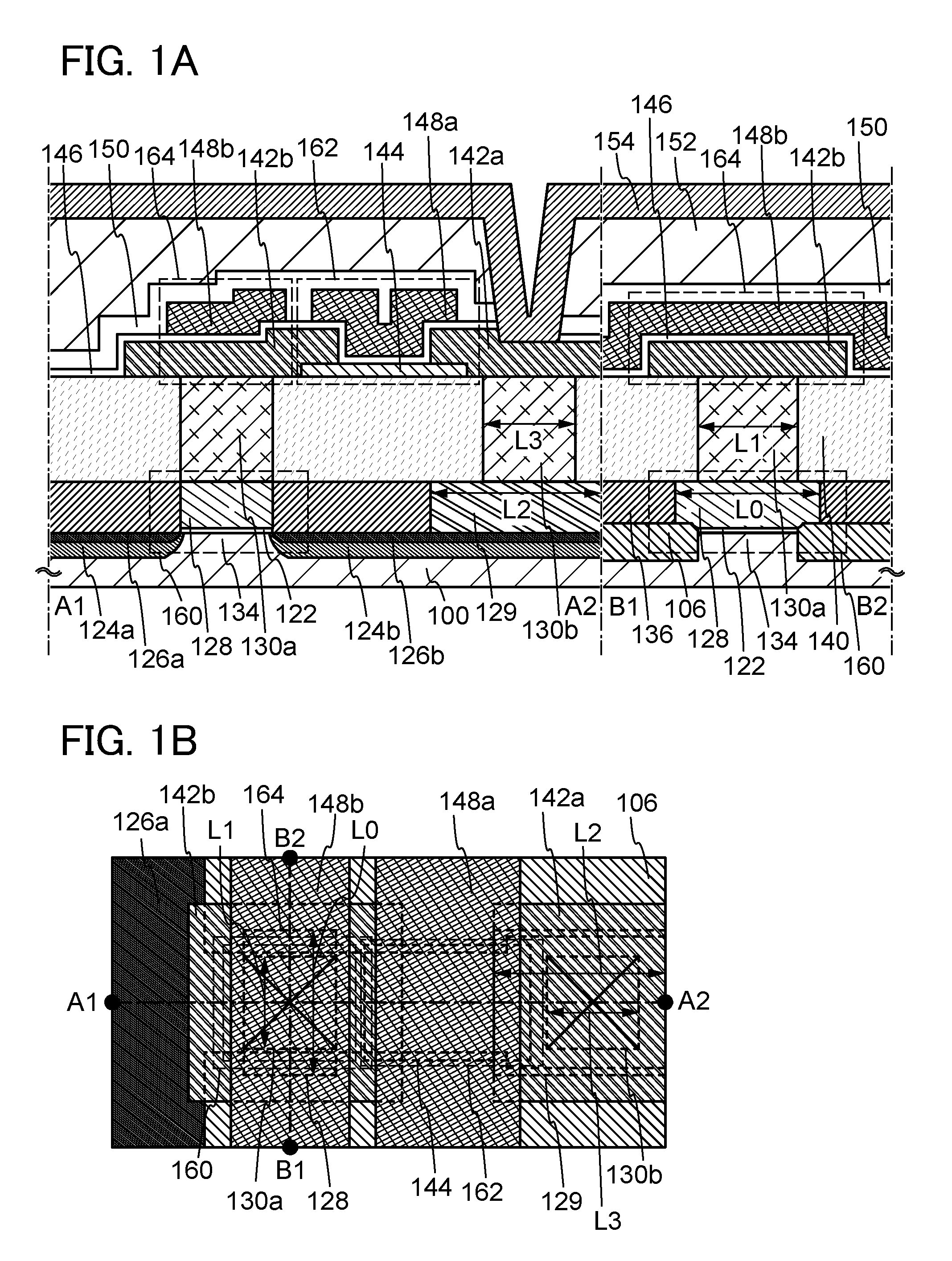
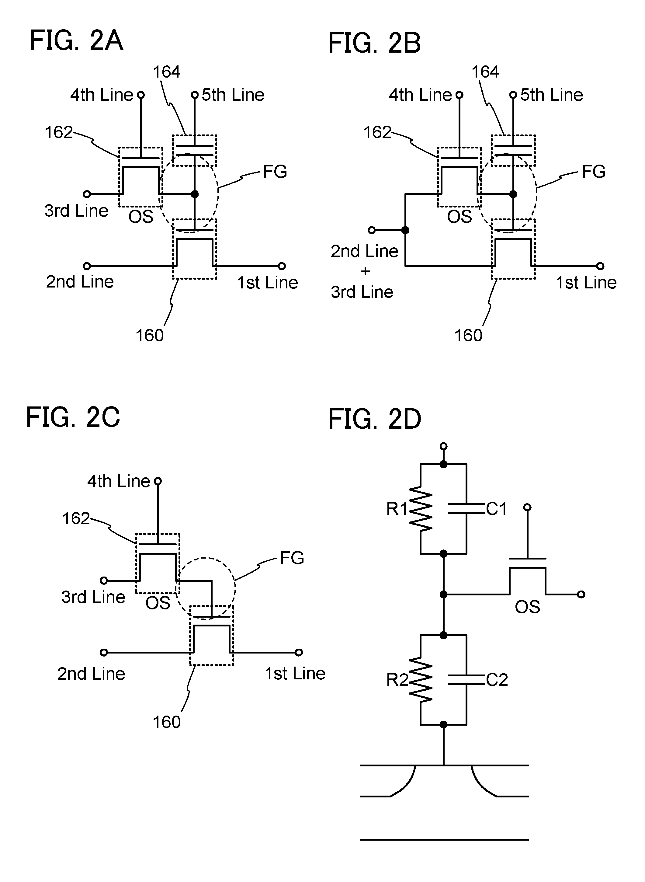
[0051]In this embodiment, the structure of a semiconductor device according to one embodiment of the present invention is described with reference to FIGS. 1A and 1B and FIGS. 2A to 2D.

[0052]FIGS. 1A and 1B illustrate a structure example of a semiconductor device. FIG. 1A is a cross-sectional view of the semiconductor device, and FIG. 1B is a plan view of the semiconductor device. Line A1-A2 in FIG. 1A corresponds to line A1-A2 in FIG. 1B, and a cross-sectional view taken along line A1-A2 in FIG. 1A illustrates the semiconductor device in a direction parallel to a channel length direction of a transistor. Further, line B1-B2 in FIG. 1A corresponds to line B1-B2 in FIG. 1B, and a cross-sectional view taken along line B1-B2 in FIG. 1A illustrates the semiconductor device in a direction perpendicular to the channel length direction of the transistor. The semiconductor device in FIGS. 1A and 1B includes a transistor 160 including a first semiconductor material in a lower portion and a t...

embodiment 2

[0116]In this embodiment, a method for forming the semiconductor device described in the above embodiment with reference to FIGS. 1A and 1B is described with reference to FIGS. 3A to 3D, FIGS. 4A to 4C, FIGS. 5A to 5D, FIGS. 6A to 6C, FIGS. 7A and 7B, and FIGS. 8A and 8B.

[0117]A method for forming the transistor 160 in a lower portion is described with reference to FIGS. 3A to 3D, FIGS. 4A to 4C, and FIGS. 5A to 5D.

[0118]First, the semiconductor substrate 100 is prepared (see FIG. 3A). A single crystal semiconductor substrate or a polycrystalline semiconductor substrate of silicon, silicon carbide, or the like; a compound semiconductor substrate of silicon germanium or the like; an SOI substrate; or the like can be used as the semiconductor substrate 100. Here, an example in which a single crystal silicon substrate is used as the semiconductor substrate 100 is described. Note that although the term “SOI substrate” generally means a substrate where a silicon semiconductor layer is pr...

embodiment 3

[0213]In this embodiment, a structure of a semiconductor device according to one embodiment of the present invention that is different from the structure of the semiconductor device in the above embodiment is described with reference to FIGS. 9A and 9B.

[0214]FIGS. 9A and 9B illustrate a structure example of a semiconductor device. FIG. 9A is a cross-sectional view of the semiconductor device, and FIG. 9B is a plan view of the semiconductor device. Line A1-A2 in FIG. 9A corresponds to line A1-A2 in FIG. 9B, and a cross-sectional view taken along line A1-A2 in FIG. 9A illustrates the semiconductor device in a direction parallel to the channel length direction of a transistor. Further, line B1-B2 in FIG. 9A corresponds to line B1-B2 in FIG. 9B, and a cross-sectional view taken along line B1-B2 in FIG. 9A illustrates the semiconductor device in a direction perpendicular to the channel length direction of the transistor.

[0215]A transistor 260 includes a channel formation region 234 provi...


PUM


Abstract

With a combination of a transistor including an oxide semiconductor material and a transistor including a semiconductor material other than an oxide semiconductor, a semiconductor device with a novel structure in which data can be retained for a long time and does not have a limitation on the number of writing can be obtained. When a connection electrode for connecting the transistor including a semiconductor material other than an oxide semiconductor to the transistor including an oxide semiconductor material is smaller than an electrode of the transistor including a semiconductor material other than an oxide semiconductor that is connected to the connection electrode, the semiconductor device with a novel structure can be highly integrated and the storage capacity per unit area can be increased.

Description

BACKGROUND OF THE INVENTION[0001]1. Field of the Invention[0002]The disclosed invention relates to semiconductor devices including semiconductor elements and methods for manufacturing the semiconductor devices.[0003]2. Description of the Related Art[0004]Storage devices including semiconductor elements are broadly classified into two categories: volatile storage devices that lose stored data when power is not supplied and nonvolatile storage devices that retain stored data even when power is not supplied.[0005]A typical example of a volatile storage device is a dynamic random access memory (a DRAM). A DRAM stores data in such a manner that a transistor included in a storage element is selected and electric charge is accumulated in a capacitor.[0006]When data is read from a DRAM, electric charge in a capacitor is lost according to the principle; thus, another writing operation is necessary every time data is read. Further, a transistor included in a storage element has leakage curren...

Claims


Application Information

Patent Timeline
Patent Type & Authority Patents(United States)
IPC IPC(8): H01L29/78H01L29/772
CPCH01L29/78H01L27/0688H01L27/1225H01L27/1203H01L27/1156H01L29/7869G11C16/0433H01L29/408H10B41/70H01L21/02565H01L29/4236H01L29/78696
Inventor SAITO, TOSHIHIKOKATO, KIYOSHIISOBE, ATSUO
Owner SEMICON ENERGY LAB CO LTD
Why Eureka
Try Eureka