

Apparatus for jitter testing an IC
a technology of integrated circuits and apparatuses, applied in the direction of electric unknown time interval measurement, recording information storage, setting time indication, etc., can solve the problems of random jitter, data signal jitter relative to clock signal edges, data signal jitter relative to receiving ic edges, etc., to minimize delays and noise
- Summary
- Abstract
- Description
- Claims
- Application Information
AI Technical Summary
Benefits of technology
Problems solved by technology
Method used
Image

Examples
Embodiment Construction
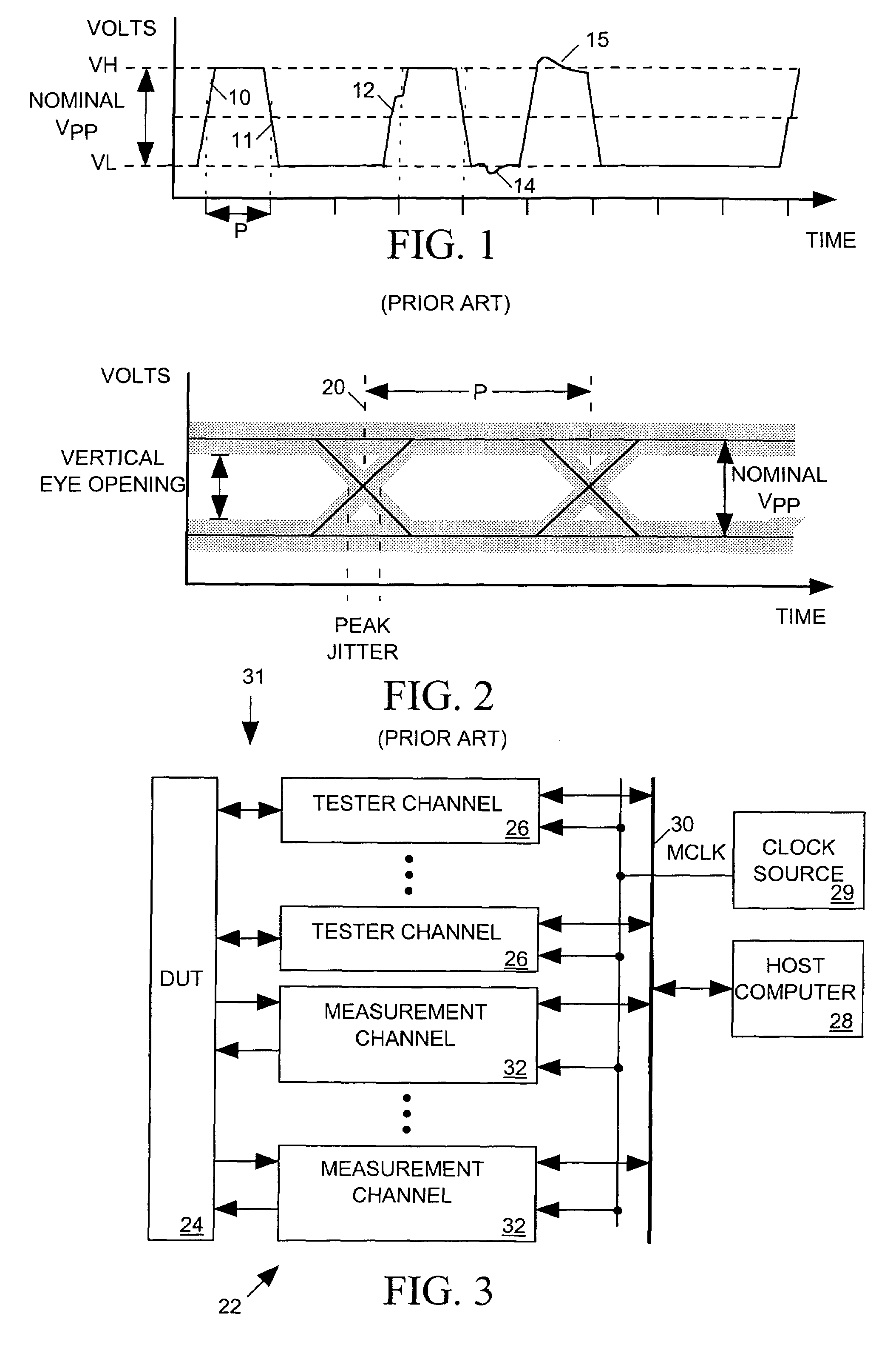
[0039]The invention relates in general to automated test equipment, and in particular to a system for testing an integrated circuit for its tolerance to jitter in its input signals and for measuring the amount of jitter in its output signals. While the specification describes in detail an exemplary embodiment of the invention considered a best mode of practicing the invention, those of skill in the art will appreciate that other modes of practicing the invention are possible.
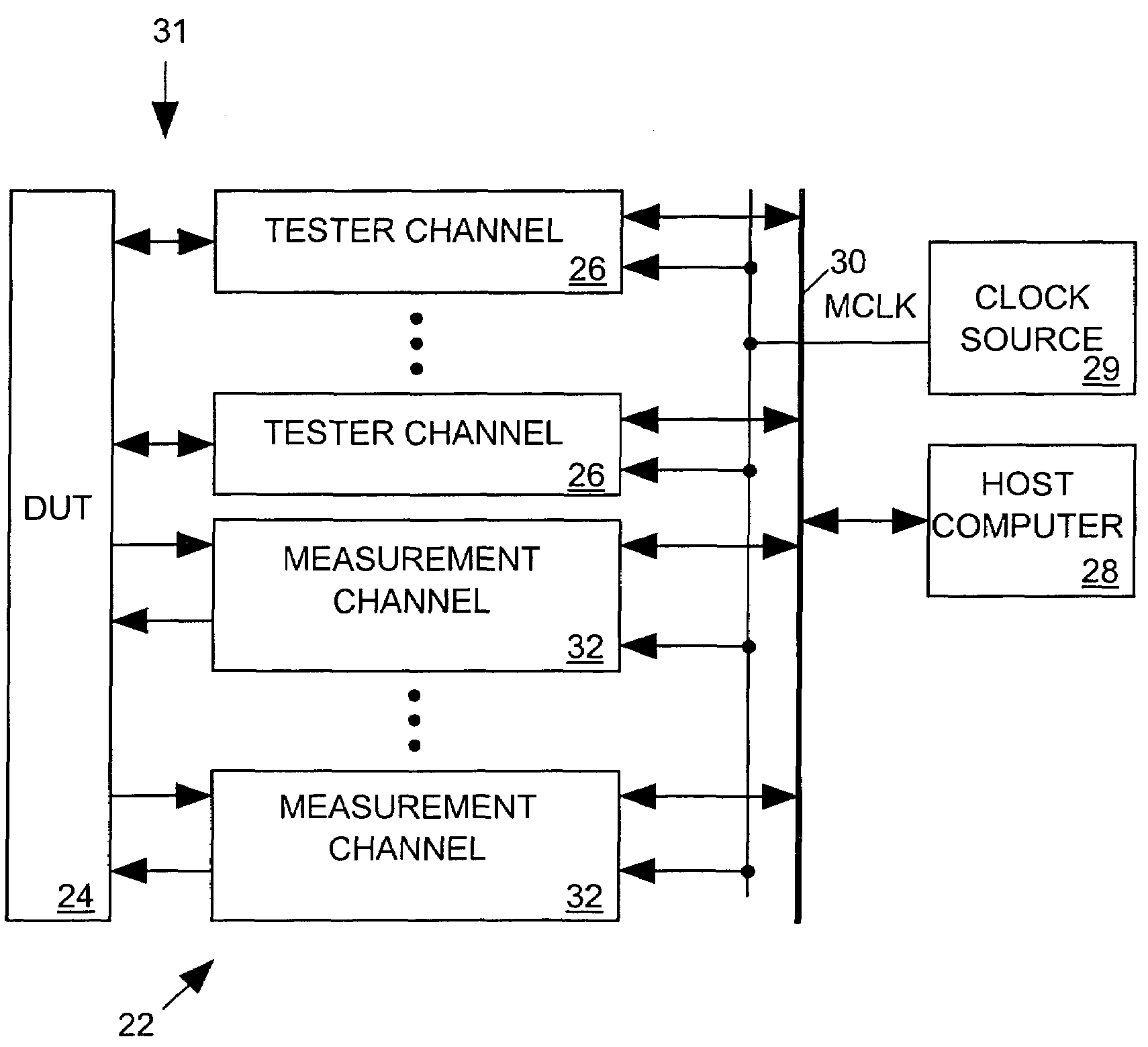
[0040]FIG. 3 depicts an integrated circuit (IC) tester 22 incorporating the present invention, including a set of conventional tester channels 26, each connected to a separate pin of an IC device under test (DUT) 24 through signal paths 31. Programmed by instructions supplied from a host computer 28 via a bus 30 and synchronized to a master clock signal MCLK produced by a clock source 29, each tester channel 26 may either transmit an input signal having a particular pattern to DUT 24 or monitor an output signal ...
PUM
 Abstract
Description
Claims
Application Information