Light-emitting element, display device, and electronic appliance

a technology of light-emitting elements and display devices, applied in the field of light-emitting elements, can solve the problems of increasing drive voltage, achieve the effect of achieving target luminance, less electric power, and high luminous efficiency

Inactive Publication Date: 2009-12-08
SEMICON ENERGY LAB CO LTD
View PDF56 Cites 10 Cited by
  • Summary
  • Abstract
  • Description
  • Claims
  • Application Information

AI Technical Summary

Benefits of technology

[0010]The present invention has been made in view of such circumstances, and it is an object of the present invention to provide an inorganic light-emitting element capable of low-voltage driving. Moreover, it is an object of the present invention to provide a display device and an electronic appliance each with reduced power consumption by using this light-emitting element.
[0028]Since the light-emitting element of the present invention has high luminous efficiency and attains target luminance with less electric power, the drive voltage can be decreased.
[0029]Further, since the display device and the electronic appliance of the present invention each include the light-emitting element having high luminous efficiency and operating at low drive voltage, the power consumption thereof can be reduced.

Problems solved by technology

This causes a problem of increase in drive voltage in a case of applying the inorganic light-emitting element to a display panel and the like.

Method used


Image

  • Light-emitting element, display device, and electronic appliance
  • Light-emitting element, display device, and electronic appliance
  • Light-emitting element, display device, and electronic appliance

Examples


embodiment mode 1

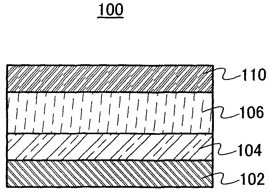
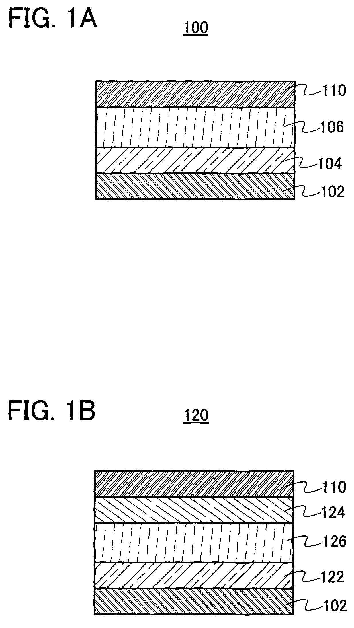
[0047]An example of a light-emitting element of the present invention is explained with reference to FIGS. 1A and 1B.

[0048]A light-emitting element 100 shown in FIG. 1A has a structure in which a first electrode 102, an electron supplying layer 104, a layer 106 containing a light-emitting substance, and a second electrode 110 are sequentially stacked. That is, in this structure, the layer 106 containing a light-emitting substance and the electron supplying layer 104 which is in contact with the layer 106 containing a light-emitting substance are interposed between the first electrode 102 and the second electrode 110.

[0049]The layer 106 containing a light-emitting substance includes a light-emitting material formed of at least a base material and an impurity element. The impurity element does not include an element included in the base material.

[0050]The base material in the layer 106 containing a light-emitting substance may be a sulfide, an oxide, or a nitride. For example, the sul...

embodiment mode 2

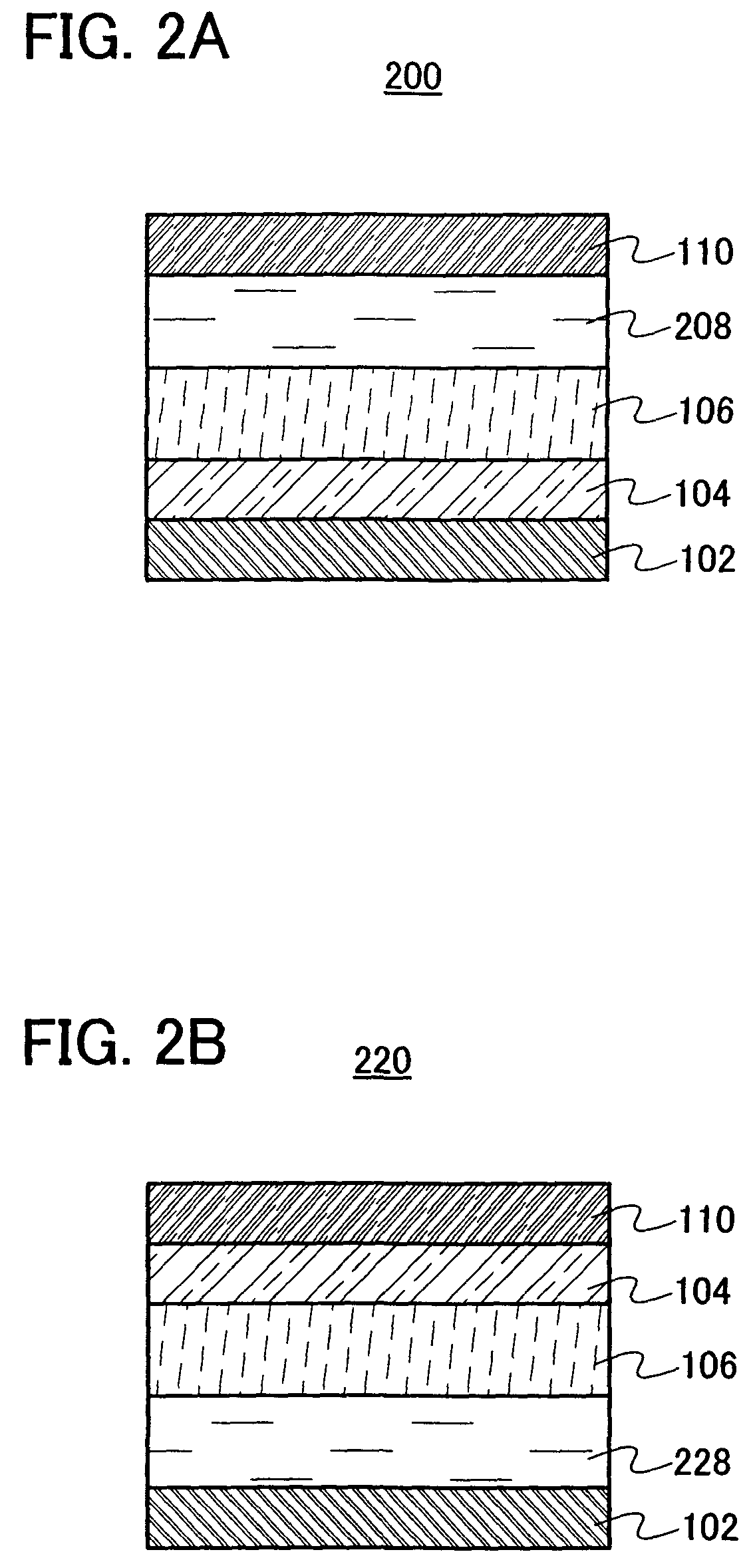
[0098]Embodiment Mode 2 will explain a light-emitting element with a different structure from that in the above embodiment mode, with reference to FIGS. 2A and 2B.

[0099]A light-emitting element 200 shown in FIG. 2A has a structure in which the first electrode 102, the electron supplying layer 104, the layer 106 containing a light-emitting substance, an insulating layer 208, and the second electrode 110 are sequentially stacked. In other words, in this structure, the layer 106 containing a light-emitting substance, the electron supplying layer 104 which is in contact with one surface of the layer 106 containing a light-emitting substance, and the insulating layer 208 which is in contact with the other surface of the layer 106 containing a light-emitting substance are interposed between the first electrode 102 and the second electrode 110.

[0100]Since the structure, the manufacturing method, and the like of the light-emitting element 200 shown in FIG. 2A except the insulating layer 208...

embodiment mode 3

[0111]Embodiment Mode 3 will explain a display device having a light-emitting element of the present invention with reference to FIGS. 4A and 4B.

[0112]The display device shown in this embodiment mode is a passive type display device in which the light-emitting element is driven without particularly providing an element for driving such as a transistor. It is to be noted that FIG. 4A is a perspective view of a passive type display device of the present invention, and FIG. 4B is a top view thereof. Specifically, FIG. 4A is a perspective view showing a portion surrounded by a dashed line 408 in FIG. 4B.

[0113]In FIG. 4A, a plurality of first electrodes 402 are provided in parallel over a first substrate 401. End portions of each of the first electrodes 402 are covered with partition wall layers 403. In order to clarify an internal structure of the display device, a second substrate 409, second electrodes 405, and a layer 404 are partially omitted in FIG. 4A. Moreover, in order to make i...


PUM


Abstract

An object is to provide an inorganic light-emitting element capable of low-voltage driving. Moreover, another object is to provide a display device and an electronic appliance with low power consumption by using this light-emitting element. The light-emitting element includes a layer containing a light-emitting substance and an electron supplying layer which is in contact with the layer containing a light-emitting substance, between a first electrode and a second electrode. The layer containing a light-emitting substance includes at least an impurity element and a base material which is a sulfide, an oxide, or a nitride. The electron supplying layer includes a substance with a lower work function than that of the base material.

Description

TECHNICAL FIELD[0001]The present invention relates to a light-emitting element utilizing electroluminescence. In addition, the present invention relates to a display device and an electronic appliance each having a light-emitting element.BACKGROUND ART[0002]In recent years, research and development have been extensively conducted on light-emitting elements utilizing electroluminescence (EL). In a basic structure of such a light-emitting element, a substance with a light-emitting property is interposed between a pair of electrodes. By application of voltage between the electrodes, light emission can be obtained from the substance with a light-emitting property.[0003]Since such a light-emitting element is of a self-light-emitting type, the light-emitting element has advantages over a liquid crystal display in that the viewing angle is wide and the visibility is high, and moreover the response speed is high and reduction in thickness and weight is possible.[0004]Light-emitting elements...

Claims


Application Information

Patent Timeline
Patent Type & Authority Patents(United States)
IPC IPC(8): H01L29/10
CPCH05B33/145H10K59/00H10K59/179H10K59/131H10K50/12H10K59/1201H05B33/14C09K11/06H10K50/00
Inventor HONDA, TATSUYA
Owner SEMICON ENERGY LAB CO LTD
Why Eureka
Try Eureka