Methods of operating p-channel non-volatile memory devices

a non-volatile memory and non-volatile technology, applied in semiconductor devices, digital storage, instruments, etc., can solve the problems of high power consumption, high power consumption, and change of status from “programmed” to “erased”, and achieve the effect of reducing potential program disturb effects and negative bias

Active Publication Date: 2009-12-22
MACRONIX INT CO LTD
View PDF71 Cites 40 Cited by
  • Summary
  • Abstract
  • Description
  • Claims
  • Application Information

AI Technical Summary

Benefits of technology

[0012]One embodiment of the present invention includes a method of programming a p-channel memory cell of the present invention by applying a positive bias to the word line of the memory cell, applying a negative bias to a bit line of the memory cell, and applying a ground bias to another bit line of the memory cell. In certain preferred embodiments, a negative bias can be applied to one or more other word lines in an array during a programming operation to reduce potential program disturb effects.

Problems solved by technology

However, certain problems are associated with conventional flash memory, such as, for example, high power consumption and program and read disturbances.
High power consumption is due to high program and erasure voltages required to induce electron tunneling for program and erase operations.
A disturbance occurs when one selected cell in the memory array is being read or programmed and another non-selected programmed memory cell sharing the same word line or bit line experiences current leakage caused by electron tunneling of the selected cell.
A loss of electrons stored in the floating gate of the non-selected memory cell may result in a change of status from “programmed” to “erased”.

Method used


Image

  • Methods of operating p-channel non-volatile memory devices
  • Methods of operating p-channel non-volatile memory devices
  • Methods of operating p-channel non-volatile memory devices

Examples


Embodiment Construction

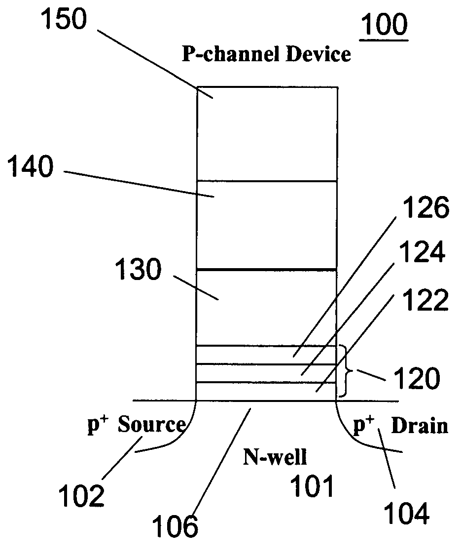
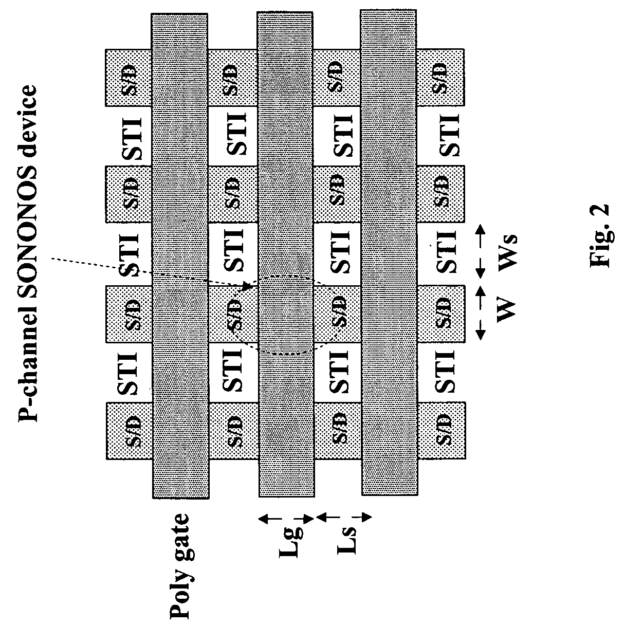
[0050]Reference will now be made in detail to the invention and the presently preferred embodiments thereof, examples of which are illustrated in the accompanying drawings. It should be noted that the non-graph drawings are in greatly simplified form and are not to precise scale. Wherever possible, the same reference numbers will be used throughout the drawings to refer to the same or like parts. In reference to the disclosure herein, for purposes of convenience and clarity only, directional terms, such as top, bottom, left, right, up, down, above, below, beneath, rear, and front, are used with respect to the accompanying drawings. Such directional terms used in conjunction with the following description of the drawings should not be construed to limit the scope of the invention in any manner not explicitly set forth in the appended claims. Although the disclosure herein refers to certain illustrated embodiments, it is to be understood that these embodiments are presented by way of ...


PUM


Abstract

Methods of operating non-volatile memory devices are described. The memory devices comprise memory cells having an n-type semiconductor substrate and p-type source and drain regions disposed below a surface of the substrate and separated by a channel region. A tunneling dielectric layer is disposed above the channel region. A charge storage layer is disposed above the tunneling dielectric layer. An upper insulating layer is disposed above the charge storage layer, and a gate is disposed above the upper insulating multi-layer structure. A positive bias is applied to a word lines of the memory device in a selected memory cell and a negative bias is applied to a bit line in the selected cell.

Description

CROSS REFERENCE TO RELATED APPLICATIONS[0001]This application is based upon and claims the benefit of, under 35 U.S.C. § 119(e), U.S. Provisional Patent Application No. 60 / 689,767, filed on Jun. 10, 2005, the entire contents of which is incorporated herein by reference.BACKGROUND OF THE INVENTION[0002]Non-volatile memory (“NVM”) refers to semiconductor memory which is able to continually store information even when the supply of electricity is removed from the device containing the NVM cell. NVM includes Mask Read-Only Memory (Mask ROM), Programmable Read-Only Memory (PROM), Erasable Programmable Read-Only Memory (EPROM), Electrically Erasable Programmable Read-Only Memory (EEPROM), and Flash Memory. Non-volatile memory is extensively used in the semiconductor industry and is a class of memory developed to prevent loss of programmed data. Typically, non-volatile memory can be programmed, read and / or erased based on the device's end-use requirements, and the programmed data can be st...

Claims


Application Information

Patent Timeline
Patent Type & Authority Patents(United States)
IPC IPC(8): G11C11/34
CPCG11C16/0475H01L27/11568H01L27/115G11C16/0483H10B69/00H10B43/30
Inventor LUE, HANG-TING
Owner MACRONIX INT CO LTD
Why Eureka
Try Eureka