

Cross-coupled oscillator, integrated circuit and electronic device
a cross-coupled oscillator and integrated circuit technology, applied in oscillator, pulse generator, pulse technique, etc., can solve problems such as cross-coupled oscillator design
- Summary
- Abstract
- Description
- Claims
- Application Information
AI Technical Summary
Benefits of technology
Problems solved by technology
Method used
Image

Examples
Embodiment Construction
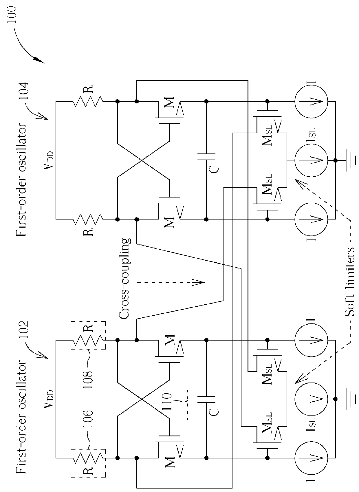
[0028]Examples of the invention will be described in terms of a cross-coupled oscillator circuit that is suitable for use with a charge pump to generate a negative bias for correctly turning off a high power RF switch. In examples of the invention, the cross-coupled oscillator circuit may be arranged to balance the duty cycle of the oscillator output by providing a complementary oscillator that employs two oscillator cores and cross-couples the output nodes of the oscillator cores, unlike the known cross-coupled oscillator architecture of FIG. 1 that uses current feedback between cores to generate quadrature signals. Examples of the invention will also be described in terms of a series-connected cross-coupled oscillator circuit, whereby the oscillator cores of the oscillator circuit share the same supply, but with different potentials, unlike known cross-coupled oscillator circuits that may share the same supply but also share the exact same potentials. In this manner, the oscillato...
PUM
 Abstract
Description
Claims
Application Information