Semiconductor architecture having field-effect transistors especially suitable for analog applications
What is AI technical title?
AI technical title is built by Patsnap AI team. It summarizes the technical point description of the patent document.
a field-effect transistor and semiconductor technology, applied in the field of semiconductor technology, can solve the problems of many requirements imposed on analog igfet performance that conflict with the results of digital scaling, the operation of the igfet cannot be controlled with the gate electrode, and the weakened analog performance, etc., to achieve excellent analog performance and low parasitic capacitance
Active Publication Date: 2010-01-05
NAT SEMICON CORP
View PDF12 Cites 50 Cited by
Summary
Abstract
Description
Claims
Application Information
AI Technical Summary
This helps you quickly interpret patents by identifying the three key elements:
Problems solved by technology
Method used
Benefits of technology
Benefits of technology
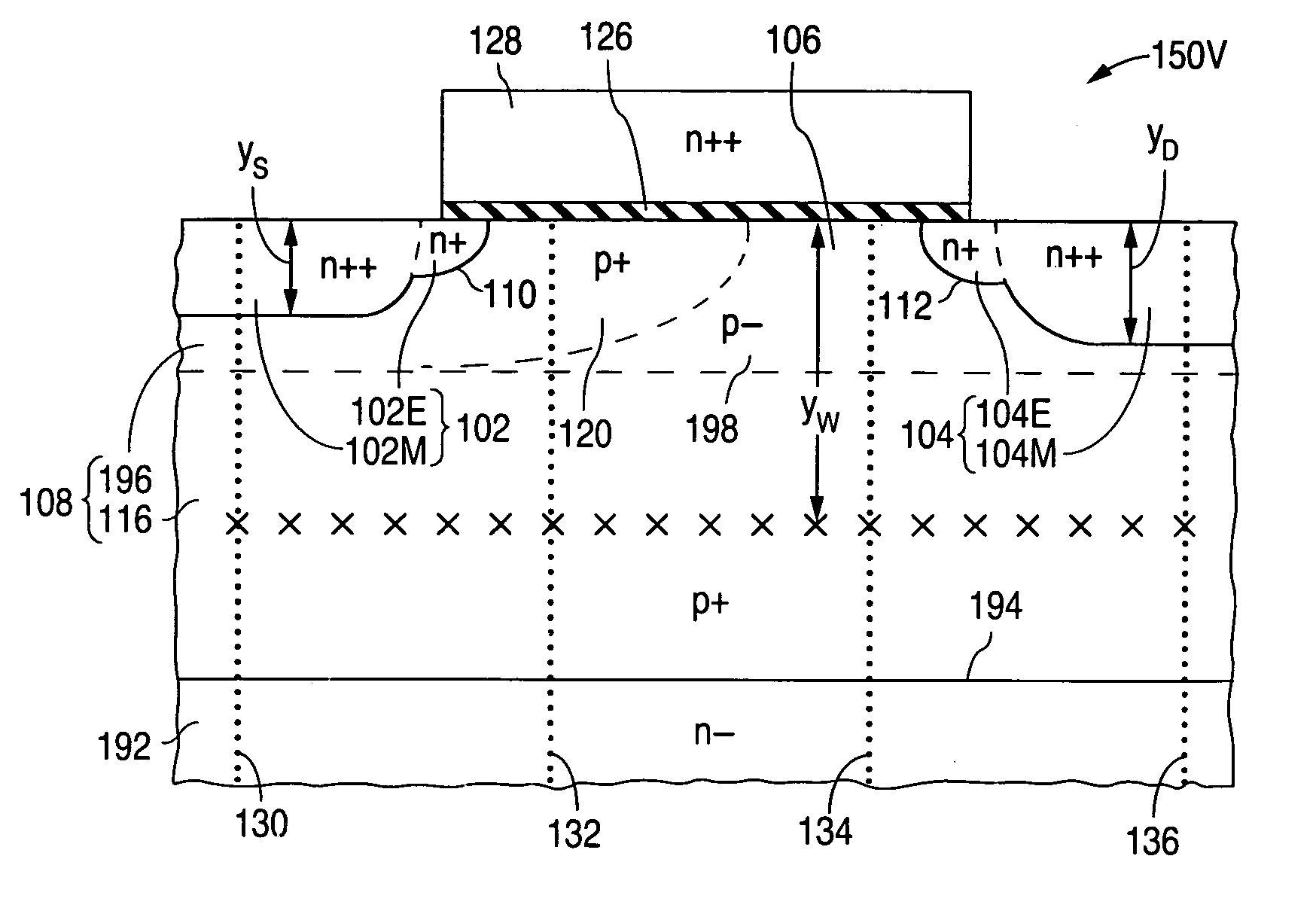
[0026]The present invention provides such an architecture. In accordance with the invention, a semiconductor structure contains a principal IGFET having comparatively low parasitic capacitance along at least one of the pn junctions that form source / drain boundaries. Although usable in digital applications, the principal IGFET is particularly suitable for analog applications and can achieve excellent analog performance.
[0029]A well portion of the body material extends below the S / D zones. The well portion is defined by semiconductor well dopant of the first conductivity type and is more heavily doped than overlying and underlying portions of the body material. Importantly, the concentration of the well dopant reaches a principal subsurface maximum along a location no more than 10 times deeper, preferably no more than 5 times deeper, below the upper semiconductor surface than a specified one of the S / D zones. This enables the concentration of all dopant of the first conductivity type in the body material to decrease by at least a factor of 10, preferably at least a factor of 20, in moving upward from the location of the subsurface maximum in the well dopant's concentration to the specified S / D zone.
[0030]Alternatively stated, the concentration of all dopant of the first conductivity type in the body material increases at least 10 times, preferably at least 20 times, in moving from the specified S / D zone downward to a body-material location no more than 10 times deeper, preferably no more than 5 times deeper, below the upper semiconductor surface than that S / D zone. This subsurface body-material location normally lies below largely all of each of the channel and S / D zones. By providing the body material with this “hypoabrupt” dopant distribution, the parasitic capacitance along the pn junction between the body material and the specified S / D zone is comparatively low. The principal IGFET can thus achieve high analog performance.
[0032]The high dopant concentration along the source side of the channel zone shields the source from the comparatively high electric field in the drain because the electric field lines from the drain terminate on ionized dopant atoms which are situated in the channel zone near the source and which provide the higher channel-zone dopant concentration near the source rather than terminating on ionized dopant atoms in the depletion region along the source and detrimentally lowering the absolute value of the potential barrier for majority charge carriers coming from the source. This alleviates punchthrough. The combination of the above-mentioned hypoabrupt vertical dopant profile below the specified S / D zone, i.e., the drain here, and the increased channel-zone dopant concentration at the source side can thereby achieve high analog performance without punchthrough failure.
Problems solved by technology
When punchthrough occurs, the operation of the IGFET cannot be controlled with its gate electrode.
Although it would be economically attractive to utilize the same transistors for the analog and digital blocks, doing so would typically lead to weakened analog performance.
Many requirements imposed on analog IGFET performance conflict with the results of digital scaling.
Hence, linearity demands on analog transistors are very high.
Because the resultant dimensional spreads are inherently large, parameter matching in digital circuitry is often relatively poor.
Method used
Image
Click on the blue label to locate the original text in one second.
Reading with bidirectional positioning of images and text.
Examples
Embodiment Construction
Reference Notation and Other Conventions
[0107]The reference symbols employed below and in the drawings have the following meanings where the adjective “lineal” means per unit IGFET width and where the adjective “areal” means per unit lateral area:
[0108]
AI ≡current gainCda ≡areal depletion-region capacitanceCd0a ≡value of areal depletion-region capacitance at zero reverse voltageCDB ≡drain-to-body capacitanceCDBw ≡lineal drain-to-body capacitanceCGB ≡gate-to-body capacitanceCGD ≡gate-to-drain capacitanceCGIa ≡areal gate dielectric capacitanceCGS ≡gate-to-source capacitanceCL ≡load capacitanceCSB ≡source-to-body capacitanceCSBw ≡lineal source-to-body capacitancef ≡frequencyfT ≡cut-off frequencyfTpeak ≡peak value of cut-off frequencygm ≡intrinsic transconductance of IGFETgmw ≡lineal transconductance of IGFETgmb ≡transconductance of body electrodegmeff ≡effective transconductance of IGFET in presence of source resistancegmsatw ≡lineal transconductance of IGFET at saturationHA ≡amplifier...
PUM
Abstract
An insulated-gate field-effect transistor (100, 100V, 140, 150, 150V, 160, 170, 170V, 180, 180V, 190, 210, 210W, 220, 220U, 220V, 220W, 380, or 480) has a hypoabrupt vertical dopant profile below one (104 or 264) of its source / drain zones for reducing the parasitic capacitance along the pn junction between that source / drain zone and adjoining body material (108 or 268). In particular, the concentration of semiconductor dopant which defines the conductivity type of the body material increases by at least a factor of 10 in moving from that source / drain zone down to an underlying body-material location no more than 10 times deeper below the upper semiconductor surface than that source / drain zone. The body material preferably includes a more heavily doped pocket portion (120 or 280) situated along the other source / drain zone (102 or 262). The combination of the hypoabrupt vertical dopant profile below the first-mentioned source / drain zone, normally serving as the drain, and the pocket portion along the second-mentioned source / drain zone, normally serving as the source, enables the resultant asymmetric transistor to be especially suitable for high-speed analog applications.
Description
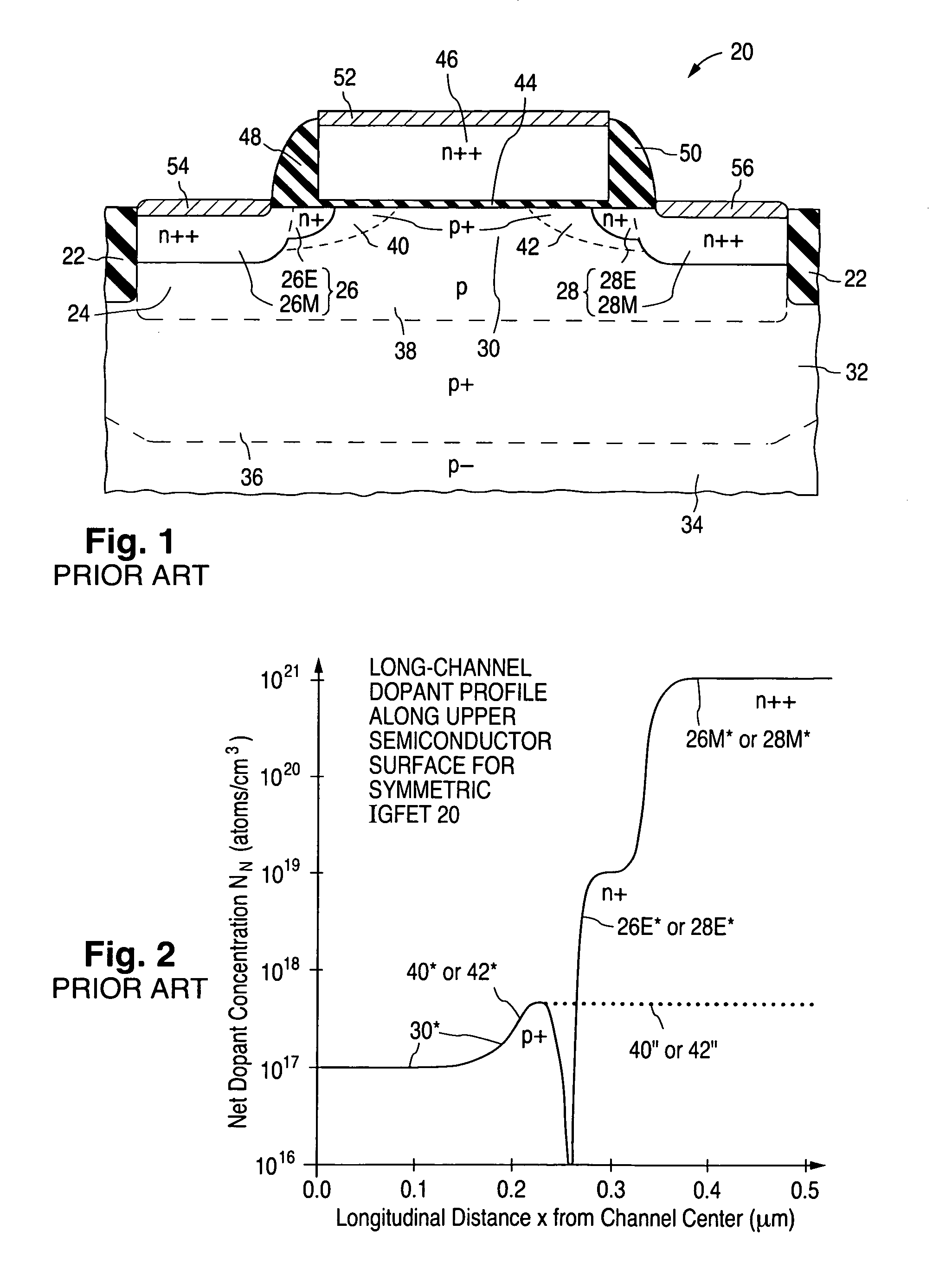
CROSS-REFERENCE TO RELATED APPLICATIONS[0001]This is a continuation-in-part of U.S. patent application Ser. No. 11 / 977,213, filed 23 Oct. 2007, which is a division of U.S. patent application Ser. No. 11 / 215,537, filed 29 Aug. 2005, now U.S. Pat. No. 7,419,863 B1. This is also related to co-filed U.S. patent application Ser. No. 11 / 981,355. All of the material in U.S. applications Ser. Nos. 11 / 215,537 and, 11 / 981,355 is incorporated by reference herein to the extent not expressly repeated herein.FIELD OF USE[0002]This invention relates to semiconductor technology and, in particular, to field-effect transistors (“FETs”) of the insulated-gate type. All of the insulated-gate FETs (“IGFETs”) described below are surface-channel enhancement-mode IGFETs except as otherwise indicated.BACKGROUND[0003]An IGFET is a semiconductor device in which a gate dielectric layer electrically insulates a gate electrode from a channel zone extending between a source zone and a drain zone. The channel zone ...
Claims
Application Information
Patent Timeline
Application Date:The date an application was filed.
Publication Date:The date a patent or application was officially published.
First Publication Date:The earliest publication date of a patent with the same application number.
Issue Date:Publication date of the patent grant document.
PCT Entry Date:The Entry date of PCT National Phase.
Estimated Expiry Date:The statutory expiry date of a patent right according to the Patent Law, and it is the longest term of protection that the patent right can achieve without the termination of the patent right due to other reasons(Term extension factor has been taken into account ).
Invalid Date:Actual expiry date is based on effective date or publication date of legal transaction data of invalid patent.

