

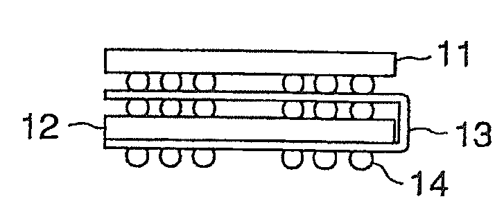
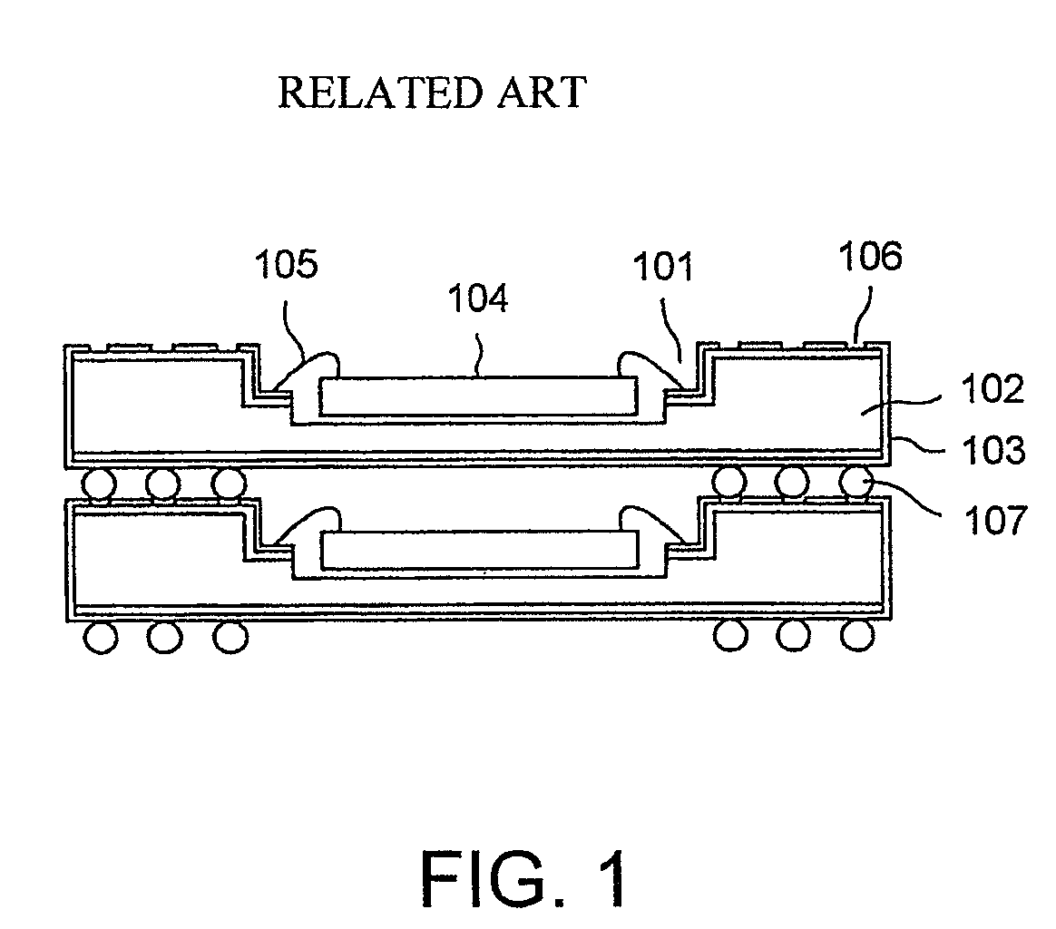
Stacked semiconductor package
a technology of semiconductor packages and stacking, applied in the direction of semiconductor devices, semiconductor/solid-state device details, electrical devices, etc., can solve the problem of different distances from external connection terminals
- Summary
- Abstract
- Description
- Claims
- Application Information
AI Technical Summary
Benefits of technology
Problems solved by technology
Method used
Image

Examples
Embodiment Construction
[0045]Now, a preferred embodiment of this invention will be described in detail with reference to the drawings.
[0046]Referring to FIGS. 4A and 4B, a stacked semiconductor package 10 according to one embodiment of this invention comprises a first semiconductor chip 11, a second semiconductor chip 12, and a flexible substrate 13 on which the first and the second semiconductor chips 11 and 12 are mounted. The flexible substrate 13 has top and bottom surfaces as first and second surfaces opposite to each other.
[0047]The first semiconductor chip 11 is mounted on the top surface of the flexible substrate 13 in a chip mounting area (51 in FIG. 11) as one of two areas defined by dividing the top surface into two halves. The second semiconductor chip 12 is mounted on the bottom surface of the flexible substrate 13 to face the first semiconductor chip 11 with the flexible substrate 13 interposed therebetween. The first and the second semiconductor chips 11 and 12 are mounted to the flexible s...
PUM
 Abstract
Description
Claims
Application Information