Device

a technology of semiconductors and devices, applied in the field of semiconductor devices, can solve the problems of consuming a lot of power and the dll circuit mounted on each chip, and achieve the effect of eliminating the need for processing and high-speed data transmission

Active Publication Date: 2013-04-18
LONGITUDE LICENSING LTD
View PDF2 Cites 20 Cited by
  • Summary
  • Abstract
  • Description
  • Claims
  • Application Information

AI Technical Summary

Benefits of technology

[0005]It is desirable that in a semiconductor device having a plurality of controlled chips stacked on a control chip, all data signals transmitted from the controlled chips to the control chip are synchronized with the same clock signal when received by the control chip. This is because this eliminates the need of processing to synchronize the data received by the control chip with the clock signal and enables high-speed data transmission.

Problems solved by technology

Furthermore, this configuration, having a DLL circuit mounted on each chip, consumes a lot of power.

Method used


Image

  • Device
  • Device
  • Device

Examples


Embodiment Construction

[0021]A representative example of a technical concept of the invention to solve the problem will be described below. It should be understood, however, that what is claimed in this application is not limited to the technical concept described herein but is defined only by the appended claims.

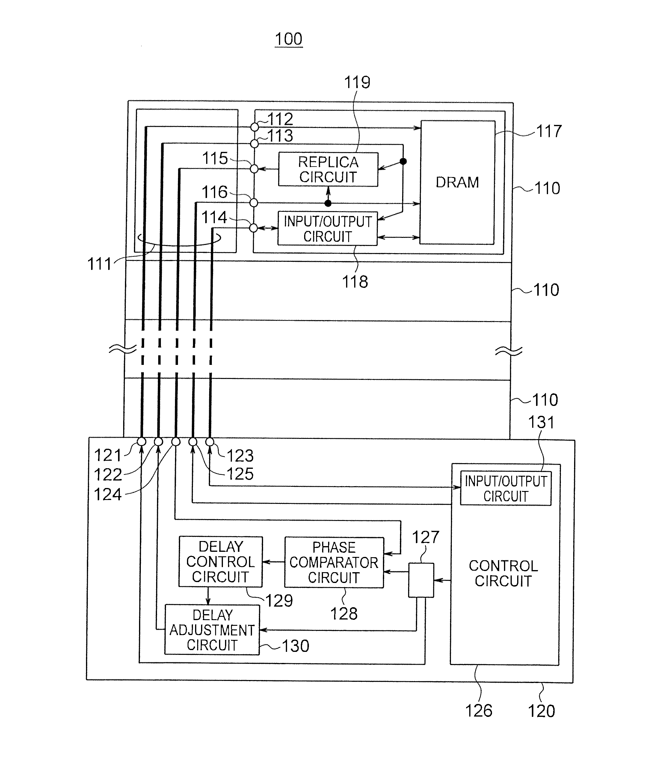
[0022]FIG. 1 shows a schematic configuration of a semiconductor device 100 according to an example of the technical concept of the invention.

[0023]The semiconductor device 100 has a plurality of controlled chips 110 and a control chip 120 for controlling them. The controlled chips 110 are stacked on one another, while they are stacked on the control chip 120.

[0024]A circuit related to a DLL circuit included in the semiconductor device 100 is characterized as follows. The control chip 120 has a first control circuit 126 which outputs a synchronization signal and receives a data signal. There are arranged, in this control chip 120, a delay adjustment circuit 130 which delays a synchronization signa...


PUM


Abstract

A semiconductor device includes a first controlled chip and a control chip stacked therewith. The first controlled chip includes a first circuit outputting a data signal in response to a synchronization signal, an input/output circuit outputting the data signal to a data terminal in synchronization with a delayed synchronization signal, and a replica circuit replicating an output circuit and outputting a replica signal to a first replica terminal in synchronization with the delayed synchronization signal. The control chip includes a first control circuit outputting a synchronization signal and receiving a data signal, a delay adjustment circuit delaying the synchronization signal and outputting the same as a delayed synchronization signal, a phase comparator circuit comparing the phases of the replica signal and the synchronization signal, and a delay control circuit controlling the delay amount of the delay adjustment circuit based on a comparison result of the phase comparator circuit.

Description

[0001]This application claims priority to prior Japanese application JP 2011-228532, the disclosure of which is incorporated herein by reference.BACKGROUND OF THE INVENTION[0002]This invention relates to a semiconductor device including a plurality of chips, and in particular to a semiconductor device having DLL (Delay Locked Loop) circuits.[0003]Japanese Patent Application Publication No. 2011-029535 (Patent Document 1) discloses a semiconductor device of a COC (Chip On Chip) structure having a plurality of stacked semiconductor chips, in which a DLL circuit is mounted on each of the semiconductor chips (see FIG. 3).[0004]Japanese Patent Application Publication No. 2008-065884 (Patent Document 2) discloses a semiconductor device of a MCM (Multi Chip Module) structure in which a clock signal is transmitted from a DLL circuit of a first chip to a second chip (See FIG. 1). A similar configuration is described also in Japanese Patent Application Publication No. 2006-013495 (Patent Docu...

Claims


Application Information

Patent Timeline
Patent Type & Authority Applications(United States)
IPC IPC(8): H03L7/097G11C5/06
CPCG11C11/4076G11C11/4093H01L2924/1305H01L2924/13091H03L7/097G11C11/4096G11C5/063G11C11/40G11C29/023G11C29/028H03L7/0812G11C7/1066G11C7/1093G11C7/222H01L25/0657G11C11/4063H01L2224/16145H01L2924/00H03L7/0814H03L7/0816
Inventor RIHO, YOSHIRO
Owner LONGITUDE LICENSING LTD
Why Eureka
Try Eureka