FPGA (field programmable gate array) based USB3.0 interface module

An interface module and interface technology, applied in the field of USB 3.0 interface modules, can solve the problems of large Ethernet transmission delay, PCI bus does not support hot plugging, and low USB2.0 transmission rate, etc.

Inactive Publication Date: 2015-09-02
HARBIN INST OF TECH
View PDF1 Cites 21 Cited by
  • Summary
  • Abstract
  • Description
  • Claims
  • Application Information

AI Technical Summary

Problems solved by technology

Due to the low transmission rate of USB 2.0, the highest is only 480Mbps, the PCI bus does not support hot plugging and is limited to desktop computers, and the transmission delay of Ethernet is very large

Method used


Image

  • FPGA (field programmable gate array) based USB3.0 interface module
  • FPGA (field programmable gate array) based USB3.0 interface module
  • FPGA (field programmable gate array) based USB3.0 interface module

Examples


specific Embodiment approach 1

[0059] Specific implementation mode 1. Combination Figure 1 to Figure 10 Illustrate this specific implementation mode, the USB 3.0 interface module based on FPGA,

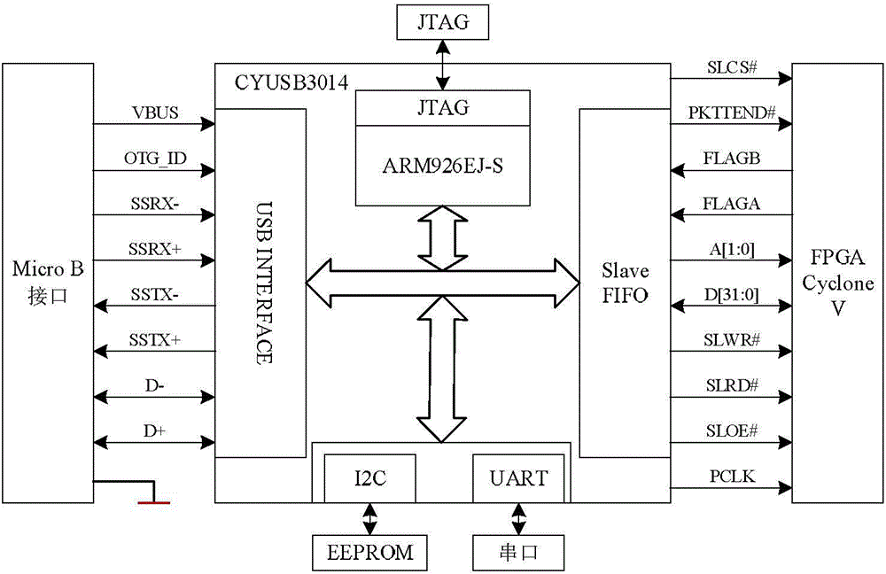
[0060] The present invention is based on the USB 3.0 peripheral controller FX3 series chip CYUSB3014 of CYPRESS Company, uses Altera Company's FPGA as the main control chip to control the read and write timing of the FX3 chip, and aims to realize the USB 3.0 high-speed interface, and designs a maximum up to 2.5 Data transfer interface with Gbps transfer rate.

[0061] 1. Hardware circuit

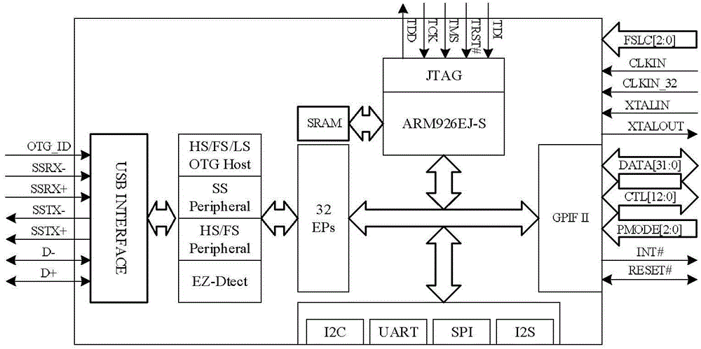
[0062] The FX3 series CYUSB3014 chip of CYPRESS has become the mainstream choice of USB 3.0 peripheral controllers because of its highly integrated and flexible features. FX3 integrates a 32-bit ARM926EJ-S microprocessor with a working frequency of 200MHz and powerful data processing capabilities. The chip integrates USB 3.0 and USB 2.0 physical layers, and provides SPI, I2C, UART and I2S interfaces to communicate with extern...

specific Embodiment

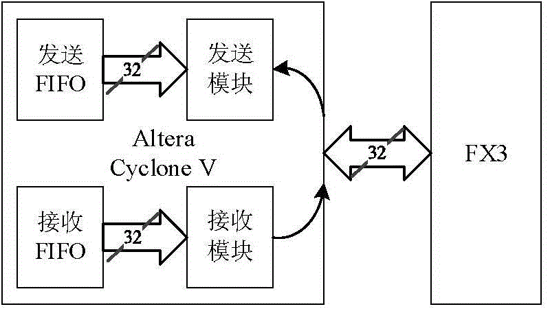
[0111] 1. Sending channel:

[0112] 1), the host software provided by CYPRESS company sends data;

[0113] 2), the FX3 chip firmware program receives the data sent by the host software and writes it into the slave device FIFO;

[0114] 3), the USB 3.0 firmware program outputs the sending status to the USB 3.0 interface logic;

[0115] 4), the USB 3.0 interface logic sending module enters the state transition, and detects the FX3 firmware state;

[0116] 5), the USB 3.0 interface logic sending module reads data from the device FIFO from the FX3 chip;

[0117] 2. Receive channel:

[0118] 1), the host software provided by CYPRESS company sends and receives the request;

[0119] 2), the USB 3.0 firmware program outputs the receiving status to the USB 3.0 interface logic;

[0120] 3), the USB 3.0 interface logic receiving module enters the state transition and receives data;

[0121] 4), the USB 3.0 interface logic receiving module writes the received data into the FX3 chip ...


PUM


Abstract

The invention discloses an FPGA (field programmable gate array) based USB3.0 interface module, and relates to a USB3.0 interface module in order to realize compatibility with a USB2.0 high-speed interface as well as high-speed data transmission between a computer and an FPGA. According to the interface module, the FPGA is adopted to realize logic control, and the high-speed data transmission is realized through data read-write operation of synchronous slave equipment FIFO (first input first output) in a chip FX3; the interface module control logic comprises a USB3.0 transmitting module, a USB3.0 receiving module, an FIFO transmitting module for clock domain crossing operation and an FIFO receiving module for the clock domain crossing operation. The FPGA based USB3.0 ultrahigh-speed interface is compatible with the USB2.0 high-speed interface, and the high-speed data transmission between the computer and the FPGA is realized.

Description

technical field [0001] The invention relates to a USB 3.0 interface module. Background technique [0002] Computers are commonly used data storage and display devices, but their data processing capabilities are weak, which is not conducive to big data processing. With the rapid development of information technology, the explosive growth of data poses new challenges to data processing and transmission. FPGA has become an ideal platform for data processing because of its fast processing speed and large amount of data. In order to realize the data transmission between the computer and FPGA, it is necessary to design and realize a high-speed interface based on FPGA. [0003] Common interfaces for computers include USB 2.0, USB 3.0, PCI, and Ethernet. Due to the low transmission rate of USB 2.0, the highest is only 480Mbps, the PCI bus does not support hot plugging and is limited to desktop computers, while the transmission delay of Ethernet is very large. USB 3.0 has become ...

Claims


Application Information

Patent Timeline
Patent Type & Authority Applications(China)
IPC IPC(8): G06F13/40
CPCG06F13/4072G06F2213/0042
Inventor 彭宇马云彤蒙春城李攀潘大为彭喜元
Owner HARBIN INST OF TECH
Why Eureka
Try Eureka