

FPGA-based JTAG test method
A test method and test data technology, which is applied in the electronic field, can solve problems such as difficulty in determining technology, inability to judge open circuits, and inability to judge open circuits, etc., and achieve the effects of easy procurement, good accuracy, high-speed data transmission and analysis
- Summary
- Abstract
- Description
- Claims
- Application Information
AI Technical Summary
Problems solved by technology
Method used
Image

Examples
Embodiment Construction
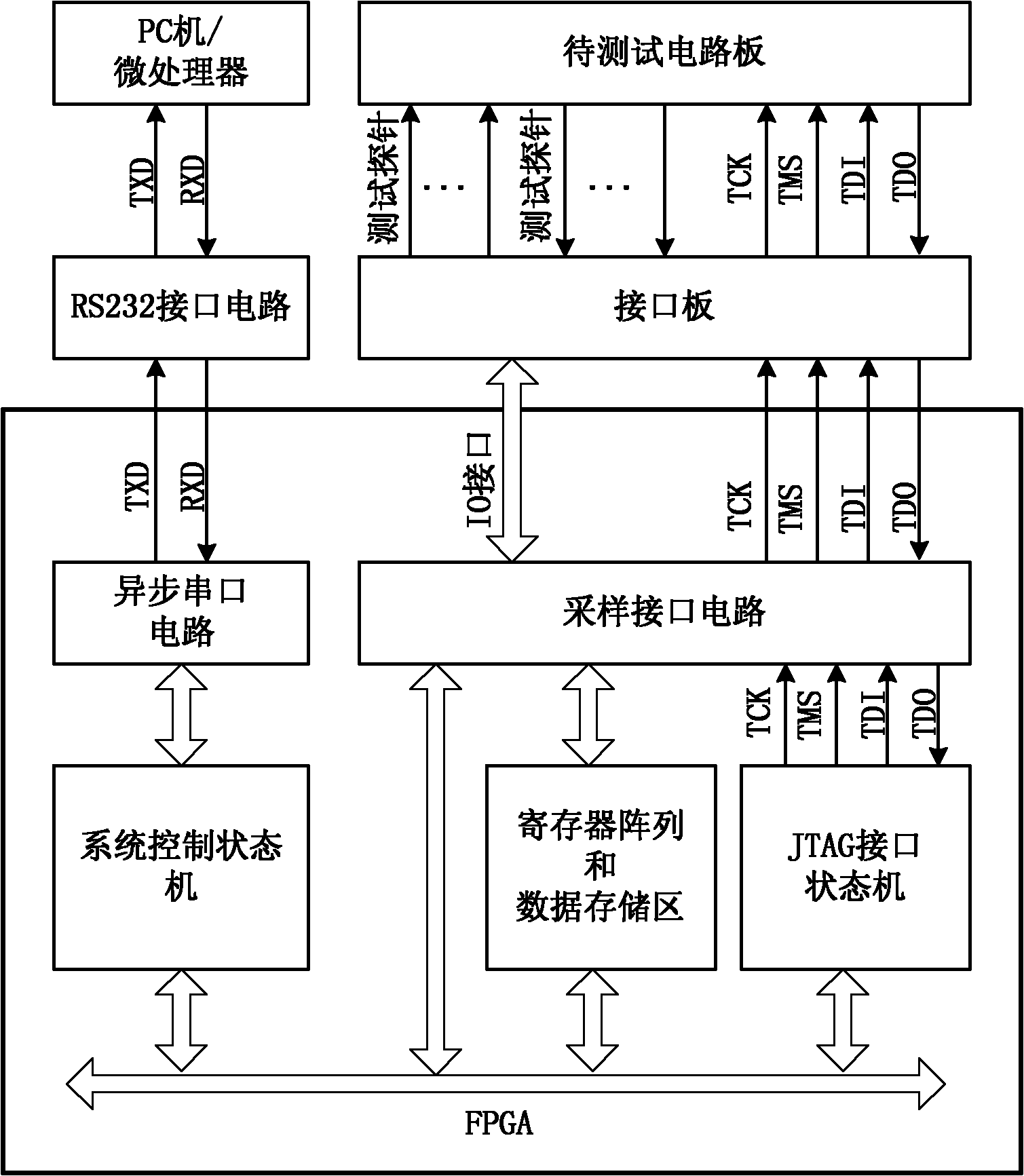
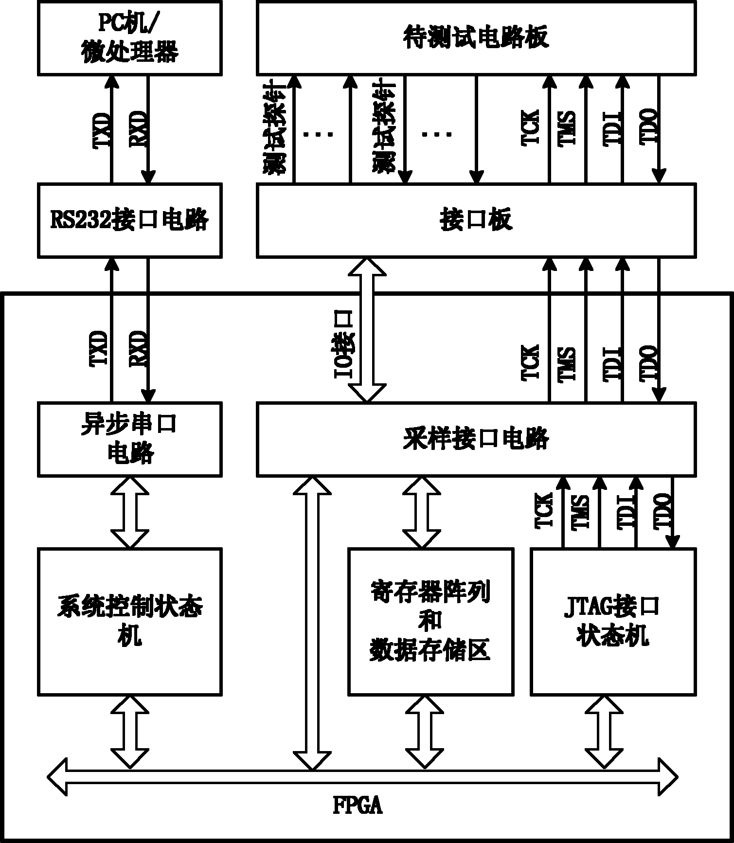
[0022] see figure 1 Shown is a schematic diagram of the interface of the JTAG test system of the present invention. figure 1 In the process, the FPGA is connected to the circuit board under test through the JTAG interface and the probes. While testing through the JTAG interface, the probes connected to the FPGA are connected to the monitoring points of the circuit board under test to read the data of each point in the test. Variety. Finally, FPGA sends data to embedded processor or PC through asynchronous serial port for data analysis and judgment. The hardware part uses VHDL language to write the whole design. Realize on FPGAEPC1E1-3T144 of LATTICE Company. The PC software part is developed by C++ software.
[0023] figure 1 Among them, the system control state machine based on FPGA realizes the analysis and execution of PC (or microprocessor) instructions. These instructions include instructions for configuring working modes, instructions for testing, and instructions f...
PUM
 Abstract
Description
Claims
Application Information