
Flash memory device and a method of manufacturing the same

a flash memory and memory technology, applied in semiconductor devices, semiconductor/solid-state device details, electrical devices, etc., can solve the problem of significant increase in and achieve the effect of minimizing the surface resistance of common source lines

Inactive Publication Date: 2010-01-19
DONGBU HITEK CO LTD
View PDF5 Cites 0 Cited by
  • Summary
  • Abstract
  • Description
  • Claims
  • Application Information

AI Technical Summary

Benefits of technology

The solution results in a flash memory device with reduced surface resistance of the source line, simplifying the manufacturing process and improving device performance by minimizing contact resistance.

Problems solved by technology

In addition, if an isolation layer is not completely removed, resistance of the common source line may be significantly increased because impurities may be non-uniformly implanted into the trench region.

Method used


Image

  • Flash memory device and a method of manufacturing the same
  • Flash memory device and a method of manufacturing the same
  • Flash memory device and a method of manufacturing the same

Examples


Embodiment Construction

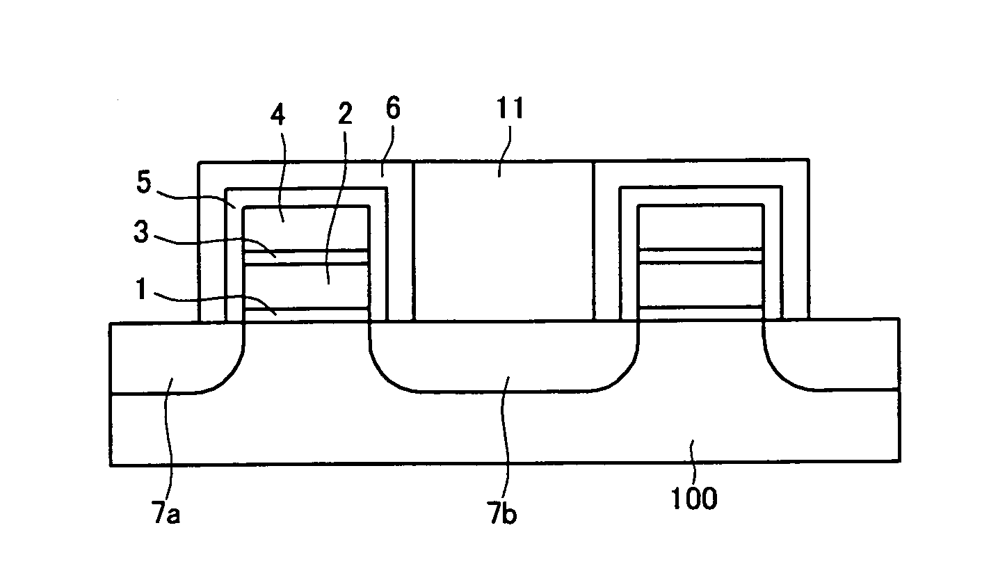
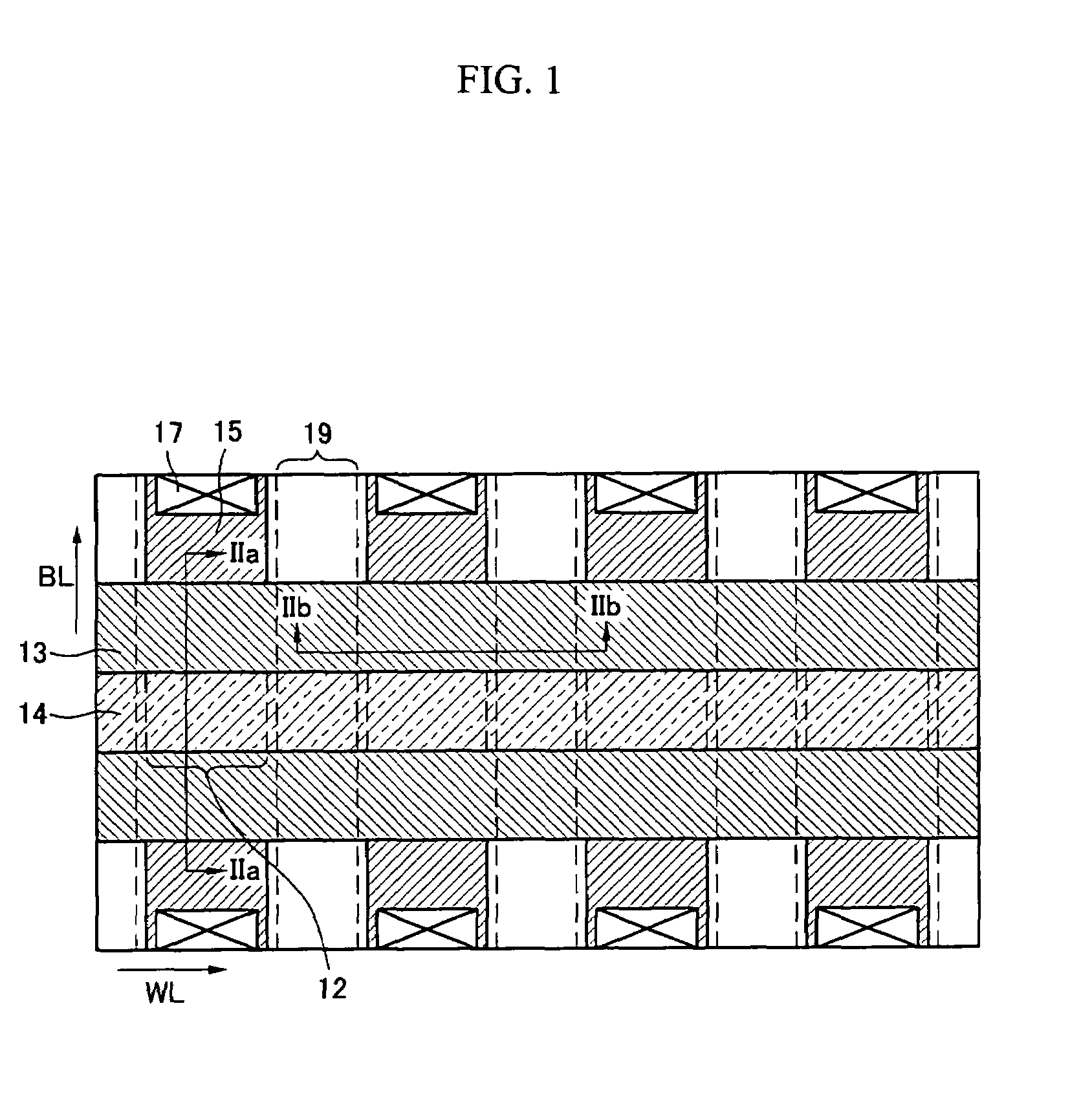
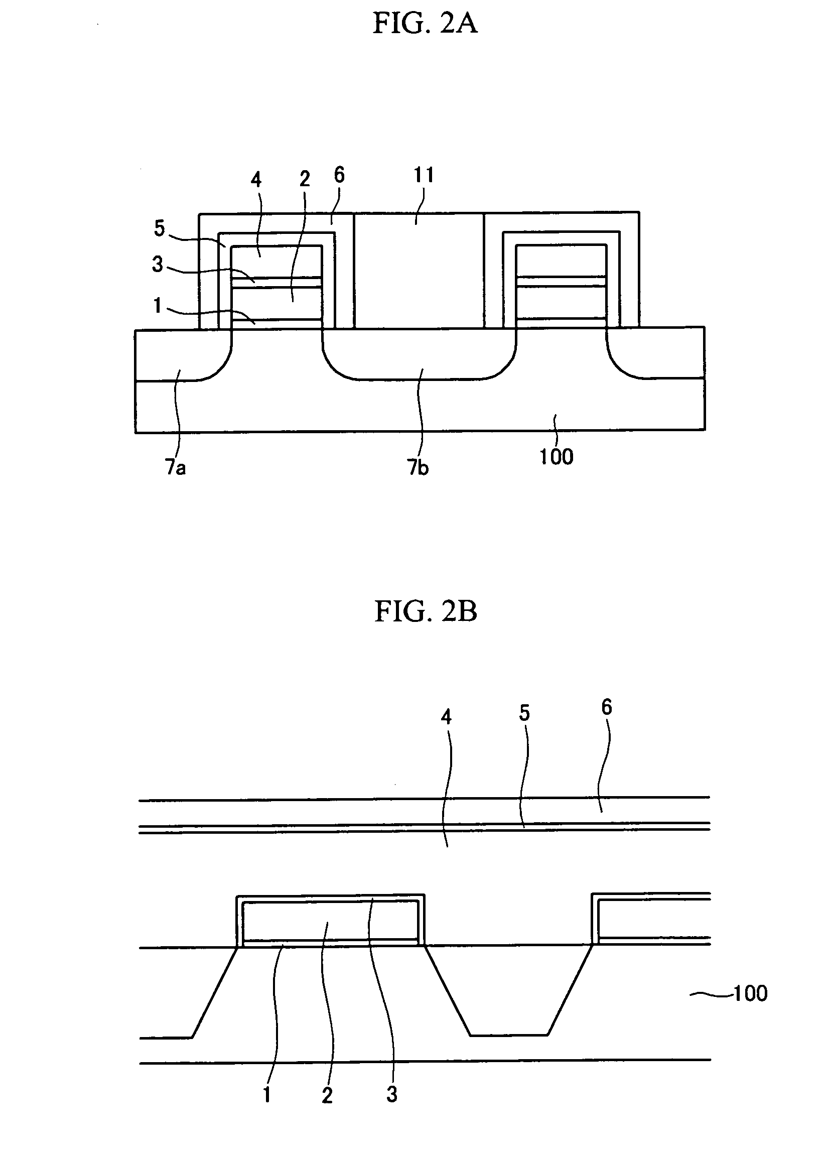
[0025]With reference to the accompanying drawings, the present invention will be described in order for those skilled in the art to be able to implement the invention. As those skilled in the art would realize, the described embodiment may be modified in various different ways, all without departing from the spirit or scope of the present invention.

[0026]To clarify multiple layers and regions, the thicknesses of the layers are enlarged in the drawings. Like reference numerals designate like elements throughout the specification. When it is said that any part, such as a layer, film, area, or plate is positioned on another part, it means that the part is directly on the other part or above the other part with at least one intermediate part. On the other hand, if any part is said to be positioned directly on another part it means that there is no intermediate part between the two parts.

[0027]Hereinafter, a flash memory cell and a method of manufacturing the same according to an exempla...


PUM


Abstract

The present invention provides a flash memory device and a method of forming the same. The method includes: forming an isolation layer and a plurality of gate lines on a semiconductor substrate; forming a source / drain region by ion-implanting impurities into the semiconductor substrate using the gate lines as a mask; forming a side oxide layer on sidewalls and surfaces of the gate lines; forming a side nitride layer on the side oxide layer; forming an insulation layer on the semiconductor substrate and the side nitride layer; forming a photosensitive layer pattern on the insulation layer; exposing the source region between the gate lines by etching the insulation layer using the photosensitive layer pattern as a mask; forming a polysilicon layer on the exposed source region and the insulation layer; and forming a source line by etching the polysilicon layer.

Description

CROSS-REFERENCE TO RELATED APPLICATION[0001]This application claims priority to and the benefit of Korean Patent Application No. 10-2005-0086099 filed in the Korean Intellectual Property Office on Sep. 15, 2005, the entire contents of which are incorporated herein by reference.BACKGROUND OF THE INVENTION[0002](a) Field of the Invention[0003]The present invention relates to a flash memory device and a method of manufacturing the same.[0004](b) Description of the Related Art[0005]Generally, a flash memory is devised to combine advantages of both EPROM (erasable programmable read only memory) and EEPROM (electrically erasable PROM), which provides a device enabling electrical data programming and erasing with a low manufacturing cost due to a simple manufacturing process and small chip size. Such a flash memory device is composed of a floating gate, a control gate, and a silicon substrate including an isolation layer, a tunnel oxide, and an insulation layer. In addition, program and er...

Claims


Application Information

Patent Timeline
Patent Type & Authority Patents(United States)
IPC IPC(8): H01L21/4763H01L29/00H10B69/00
CPCH01L27/115H01L27/11519H01L27/11521H10B41/10H10B69/00H10B41/30H01L21/3065
Inventor KIM, SUNG-JIN
Owner DONGBU HITEK CO LTD
Learn More