
Solid-state imaging device having characteristic color unit depending on color, manufacturing method thereof and camera

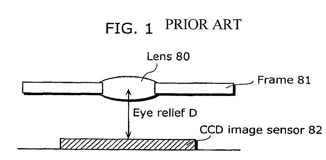
a color unit and imaging device technology, applied in the field of solid-state imaging devices and cameras, can solve the problems of color shading generation, difficult to obtain sufficient light-collecting efficiency, and worsening so as to prevent color shading generation, shorten eye relief, and increase sensitivity and color reproducibility.

Inactive Publication Date: 2010-02-02
COLLABO INNOVATIONS INC
View PDF9 Cites 13 Cited by
  • Summary
  • Abstract
  • Description
  • Claims
  • Application Information

AI Technical Summary

Benefits of technology

This approach enhances sensitivity and color reproducibility, ensures even light collection for all colors, and prevents color shading, allowing for shorter eye relief without compromising light collection, thereby improving the performance of solid-state imaging devices and cameras.

Problems solved by technology

While the microlenses are formed only on a top surface part of a chip in the conventional technology, it is getting difficult to obtain sufficient light-collecting efficiency only using the microlenses formed on the top surface part as the pixel size is further miniaturized.
Therefore, different light-collecting effects are obtained depending on the wavelengths, causing a problem of worsening the sensitivity and color reproducibility.
Further, according to the conventional technology, there is a problem that color shading is generated in the peripheral part of the imaging area as shortening the eye relief.
In other words, there is a problem that the peripheral part of the image is colored because of the collapse of the white balance.

Method used


Image

  • Solid-state imaging device having characteristic color unit depending on color, manufacturing method thereof and camera
  • Solid-state imaging device having characteristic color unit depending on color, manufacturing method thereof and camera
  • Solid-state imaging device having characteristic color unit depending on color, manufacturing method thereof and camera

Examples


first embodiment

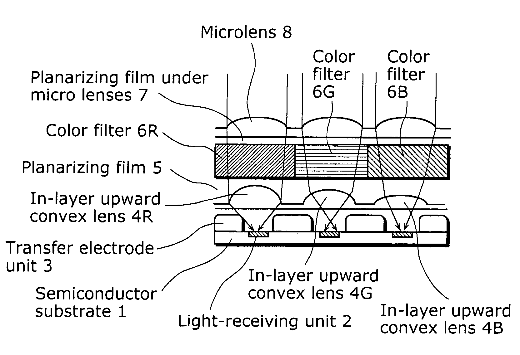
[0044]FIGS. 4A and 4B are drawings showing cross-sections of a solid-state imaging device according to an embodiment of the present invention. FIG. 4A shows a center part of an imaging area in which light-receiving units are arranged in a two-dimensional array. FIG. 4B shows a peripheral part of the imaging area. Also, arrows in the drawings indicate incident light.

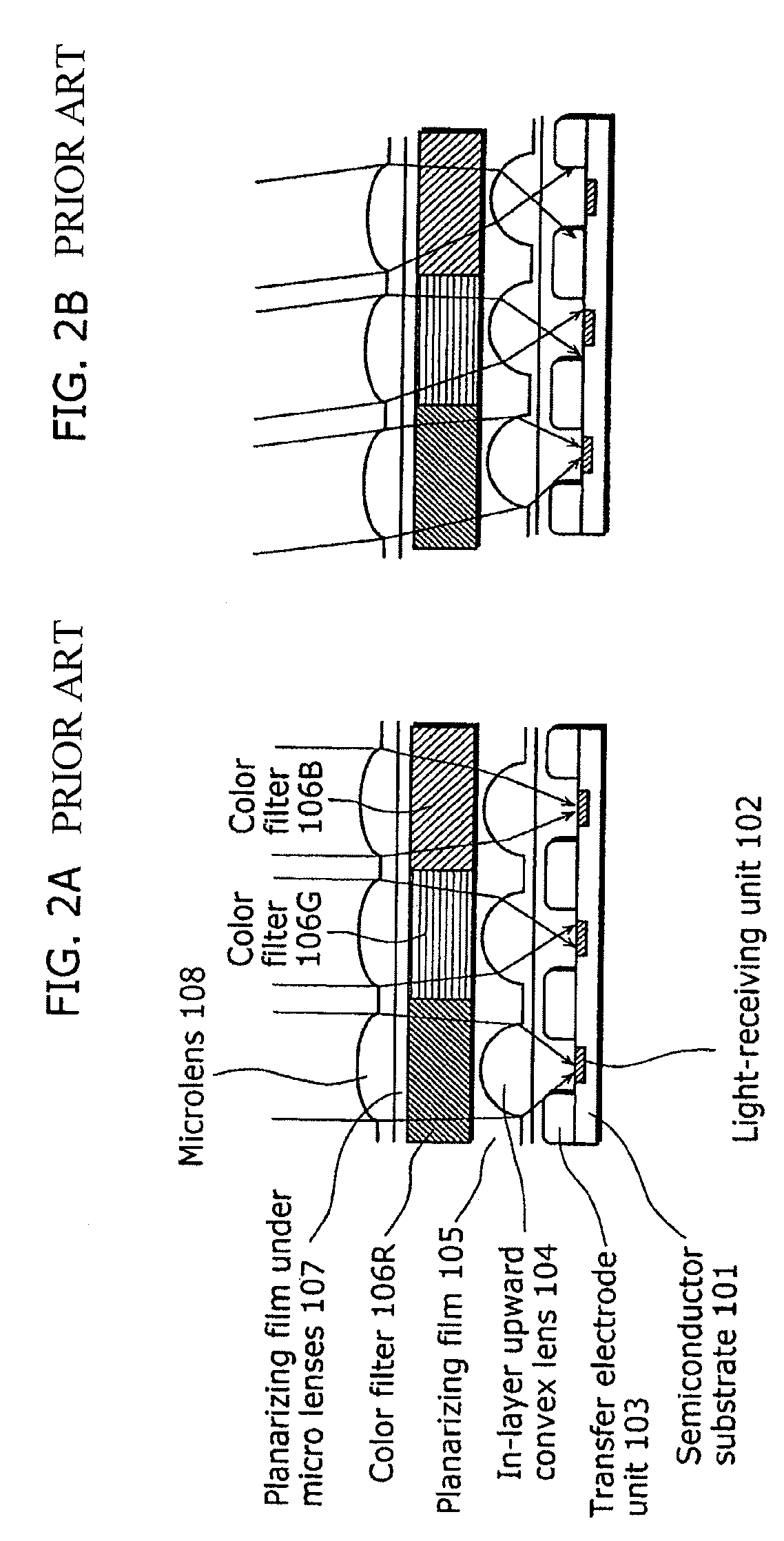
[0045]As shown in the drawings, the solid-state imaging device includes: a semiconductor substrate 1; light-receiving units 2 formed in the semiconductor layer 1; transfer electrode units 3; in-layer convex lenses 4R, 4G and 4B that are made of a plasma nitride film (refractive index n=1.9) transparent under visible light, and are different in size for respective color arrays; a planarizing film 5 made of acrylic resin (refractive index n=1.5) transparent under visible light; color filters 6R, 6G and 6B; a planarizing film 7 under microlenses; and microlenses 8 made of acrylic resin transparent under visible light. With t...


PUM


Abstract

The solid-state imaging device of the present invention includes: light-receiving units formed on a semiconductor substrate; color filters respectively formed on corresponding light-receiving units; and in-layer lenses formed above the light-receiving units and below the color filters, in which the in-layer lenses have different curvature shapes depending on colors of the corresponding color filters.

Description

BACKGROUND OF THE INVENTION[0001](1) Field of the Invention[0002]The present invention relates to a solid-state imaging device and a camera that include a semiconductor substrate having plural light-receiving units, and lenses and color filters formed inside a layer, corresponding to the respective light-receiving units.[0003](2) Description of the Related Art[0004]In recent years, with achievements of miniaturizing chip size and increasing the number of pixels of a solid-state imaging device, developments to achieve the miniaturization and high-performance of a digital camera, a digital movie camera, a camera-equipped cell phone and the like are proceeding.[0005]A conventional solid-state imaging device has light-receiving units having respective micro-lenses in order to increase sensitivity, while the chip size is miniaturized and the number of pixels is increased in the solid-state imaging device.[0006]While the microlenses are formed only on a top surface part of a chip in the c...

Claims


Application Information

Patent Timeline
Patent Type & Authority Patents(United States)
IPC IPC(8): H04N5/225H04N5/335H01L27/14H04N23/12H04N25/00H04N101/00
CPCH01L27/14625H01L27/14632H01L27/14685H04N9/045H01L27/14621H01L27/14623H01L27/14627
Inventor NISHI, YOSHIAKI
Owner COLLABO INNOVATIONS INC
Learn More