Semiconductor storage device

a technology of semiconductors and storage devices, applied in the direction of information storage, static storage, digital storage, etc., can solve the problems of large area overhead, difficult for the replica circuit to produce correct timing, and the circuit does not correctly operate, so as to achieve quick access time and relieve memory

Active Publication Date: 2010-02-02
PANASONIC SEMICON SOLUTIONS CO LTD
View PDF8 Cites 13 Cited by
  • Summary
  • Abstract
  • Description
  • Claims
  • Application Information

AI Technical Summary

Benefits of technology

[0011]Also, in a circuit configuration, such as a DRAM, that requires three memory cell operations of: 1) reading of electric charges; 2) sensing and restoring; and 3) precharging, it is desirable to increase the speed of the electric charge reading operation without significantly hindering the operating speed and access time of the whole memory cell.
[0025]As described above, according to the present invention, the timing of activating a sense amplifier for amplifying a data line having a heaviest load during a data access time (the load of a data line varies depending on the memory capacity) is logically determined, so that a quick access time can be achieved and various memory specifications can be easily achieved.

Problems solved by technology

However, in the conventional configuration, in which electric charges are used to detect the level, if the potential change does not exceed the threshold, the circuit does not correctly operate.
In this case, it is difficult for the replica circuit to produce correct timing with which a sense amplifier is activated.
Also, when a reference potential or the like is used to read out a very small potential difference, it is disadvantageously necessary to design a circuit for generating a reference potential that can reduce an influence of process variations, external conditions or the like.
There also disadvantageously occurs an area overhead due to provision of a reference circuit.

Method used


Image

  • Semiconductor storage device
  • Semiconductor storage device
  • Semiconductor storage device

Examples


first embodiment

Variation of First Embodiment

[0066]FIG. 9 is a block diagram showing a major configuration of a semiconductor storage device according to a variation of the first embodiment of the present invention. Particularly, the data line sense amplifier control signal generating logic circuit 9 is different from that of the first embodiment. FIG. 10 shows a specific circuit diagram. In FIG. 10, the data line sense amplifier control signal generating logic circuit 9 comprises a NOR circuit group 91, a dummy write buffer group 92, and an OR circuit 93, where the logical sum of a plurality of dummy data lines DDL0> to DDL serves as a control signal DACNT for a data line sense amplifier 6.

[0067]According to this variation, since the logical sum of the dummy data lines is used, even if one of the dummy memory cells is defective, data can be transferred from the remaining dummy data lines to the data line sense amplifier control signal generating logic circuit 9, so that a desired replica circuit o...

second embodiment

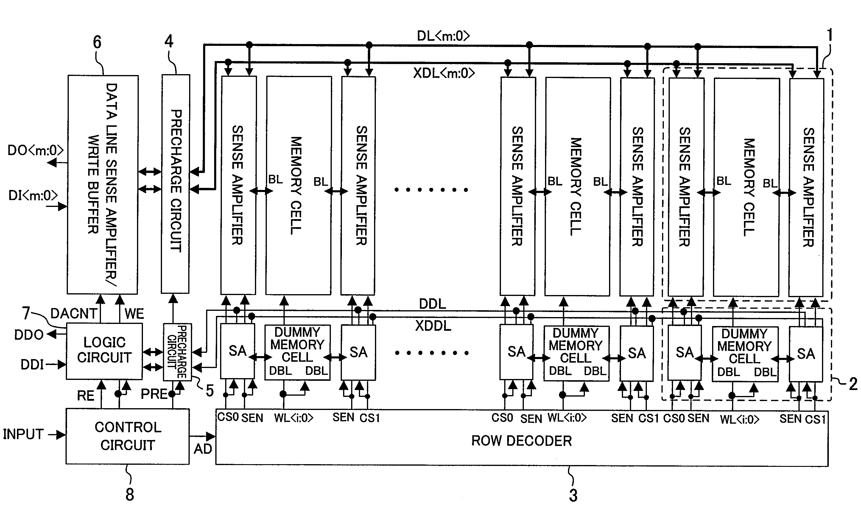
[0069]FIG. 11 is a block diagram showing a major configuration of a semiconductor storage device according to a second embodiment of the present invention. In FIG. 11, the semiconductor storage device comprises a memory array 10 and a dummy memory array 11 including a redundant word line RWL0, and a row decoder 12 including a redundant decoding circuit that can switch an access to the redundant word line RWL0 when a defect occurs in the memory array 10 and the dummy memory array 11.

[0070]In the thus-configured semiconductor storage device, if a defect occurs in a memory cell connected to a word line WL0 of the memory array 10, the address of a redundant word line is designated using, for example, a fuse function. If an access hits the defective word line WL0, the redundant decoding circuit performs a control to switch the access to the redundant word line RWL0 so that data is transferred from a redundant memory cell to a bit line BL. Thereby, the defective cell can be relieved.

[0071...

third embodiment

Variation of Third Embodiment

[0082]FIG. 13 is a block diagram showing a major configuration of a semiconductor storage device according to a variation of the third embodiment of the present invention. A data write operation to a dummy memory array 102 provided for a memory array 101 of the semiconductor storage device of FIG. 13 will be described.

[0083]A flag INT that defines a data write operation to the dummy memory array 102 is activated in a mode register 111 in accordance with an externally input control signal CNT. Thereby, a write buffer 110 is activated, so that a dummy data input signal DDI is transferred to a dummy data line DDL. Since the flag INT has H data in a selection circuit 112, an input signal DCLK in which the H level and the L level are alternated in predetermined cycles is selected, and a refresh counter 113 is counted up. An address signal selected by a count-up operation of the refresh counter 113 is decoded by a row decoder 103, and all word lines are succes...


PUM


Abstract

In a semiconductor storage device, such as a dynamic random access memory (DRAM), in which dynamic data is amplified and read on a bit line, a data line sense amplifier / write buffer connected to a data line of a memory array and a data line sense amplifier control signal generating logic circuit connected to a dummy data line of a dummy memory array are provided. A sense amplifier is activated in accordance with an output signal of the logic circuit.

Description

BACKGROUND OF THE INVENTION[0001]1. Field of the Invention[0002]The present invention relates to semiconductor storage devices, such as a dynamic random access memory (DRAM) and the like.[0003]2. Description of the Related Art[0004]In recent years, higher-speed performance is highly required for semiconductor storage devices, particularly embedded memories used in system LSIs. To achieve this, there is a known technique in which a replica circuit is used to logically determine timing with which data on a bit line read from a memory cell is amplified by a sense amplifier. This technique enables optimization of a timing margin and can also reduce influence of external conditions, process variations or the like.[0005]FIG. 15 shows a circuit configuration of a conventional DRAM including a replica circuit. The device comprises memory cells MC each including a transistor and a capacitor, word lines WL0 and WL1, bit line pairs BL0 to BLn / XBL0 to XBLn, sense amplifiers SA0 to SAn for ampli...

Claims


Application Information

Patent Timeline
Patent Type & Authority Patents(United States)
IPC IPC(8): G11C7/02
CPCG11C7/08G11C7/14G11C7/227G11C11/4099
Inventor KURODA, NAOKI
Owner PANASONIC SEMICON SOLUTIONS CO LTD
Why Eureka
Try Eureka