Semiconductor inspection system and apparatus utilizing a non-vibrating contact potential difference sensor and controlled illumination

a contact potential difference sensor and semiconductor technology, applied in the direction of individual semiconductor device testing, semiconductor/solid-state device testing/measurement, instruments, etc., can solve the problems of metal contamination not being able to be detected, system slowness, destructive, etc., to achieve the effect of easy detection and classification of surface contaminants

Inactive Publication Date: 2010-02-09
QCEPT INVESTMENTS LLC
View PDF80 Cites 4 Cited by
  • Summary
  • Abstract
  • Description
  • Claims
  • Application Information

AI Technical Summary

Benefits of technology

[0010]The system and methods provide an enhanced non-vibrating contact potential difference sensor system that allows the sensor data to be used to detect bulk semiconductor non-uniformities, or to more easily detect and classify surface contaminants. Hereinafter, semiconductor material susceptible to inspection by the system herein described will be denoted generally as a “wafer”. One embodiment includes a source of illumination that has variable intensity or spectrum of light output. The illumination source is used to illuminate the area under or near the non-vibrating contact potential difference sensor probe tip during scanning. In one embodiment, information on surface potential variations is acquired when the surface is illuminated with one or more illumination conditions that are optimized for the detection and classification of specific surface or bulk wafer characteristics that affect the response of the surface potential to illumination.

Problems solved by technology

Many of these systems are highly sensitive to specific bulk or surface characteristics, such as metallic contamination, but these systems are often slow, destructive, or make measurements at only a few points.
These systems may also be limited in the types of measurements they can make or defects that they can detect.
For example, a system which detects metal contamination may not be able to detect organic contamination, a system which can detect particles may not be able to detect sub-monolayer contaminants, or a system capable of making precise measurements at one or more points on the wafer may not be fast enough to measure all points on a wafer at production speeds.
Although multiple measurements can be made at different points on a surface, or a series of adjacent points can be measured in series, it is difficult to measure more than a few points per second.
Generating high resolution images of whole semiconductor wafers is a slow and time consuming process that is not well-suited to real-time process control applications.
These states can cause surface charging and the formation of electric fields near the surface.
Illumination of the semiconductor surface with sub-bandgap illumination can cause the population and depopulation of surface states that will also affect surface charging, band bending and the resulting surface potential.
These systems sometimes include the ability to apply controlled amounts of charge to the surface of a dielectric film.
Like the Kelvin probe, SPV measurement systems are essentially point measurement systems, and are not suitable for the generation of high resolution, whole wafer images at production speeds.
However, it is difficult to identify doping density variations using the contact potential difference signal because the effect of doping density on work function is reduced or altered by surface or interface states that induce band bending near the wafer surface.
Also, doping density variations may be difficult to separate from other non-uniformities such as variations in surface chemistry and contamination.

Method used


Image

  • Semiconductor inspection system and apparatus utilizing a non-vibrating contact potential difference sensor and controlled illumination
  • Semiconductor inspection system and apparatus utilizing a non-vibrating contact potential difference sensor and controlled illumination
  • Semiconductor inspection system and apparatus utilizing a non-vibrating contact potential difference sensor and controlled illumination

Examples


examples

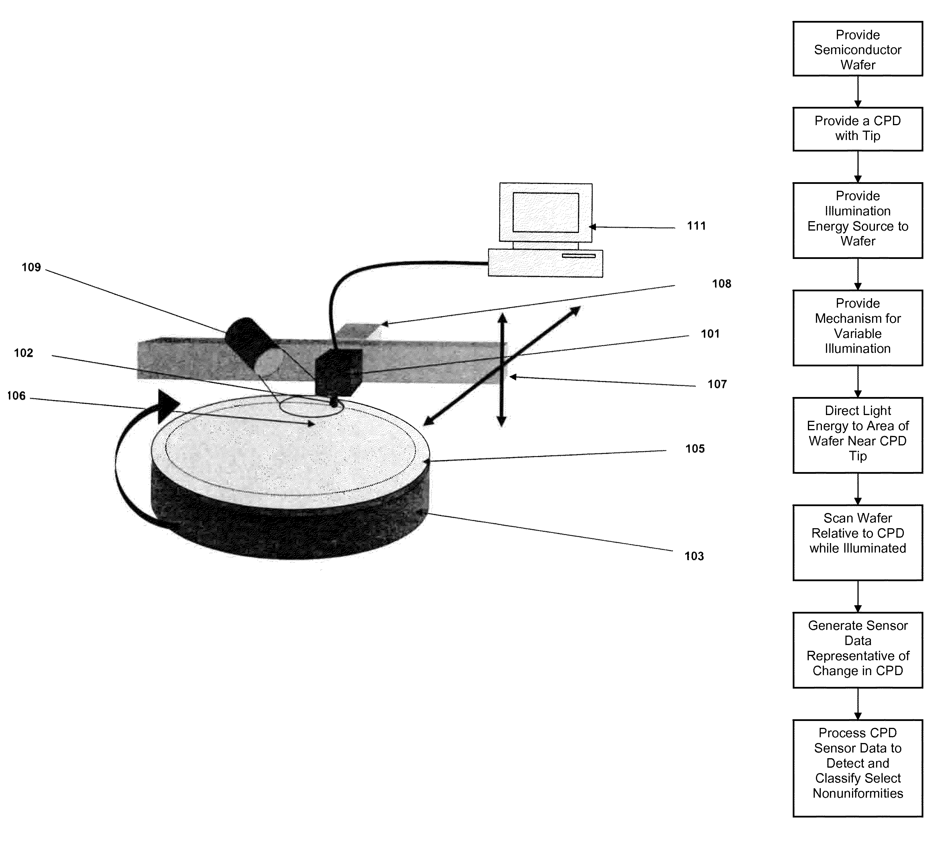
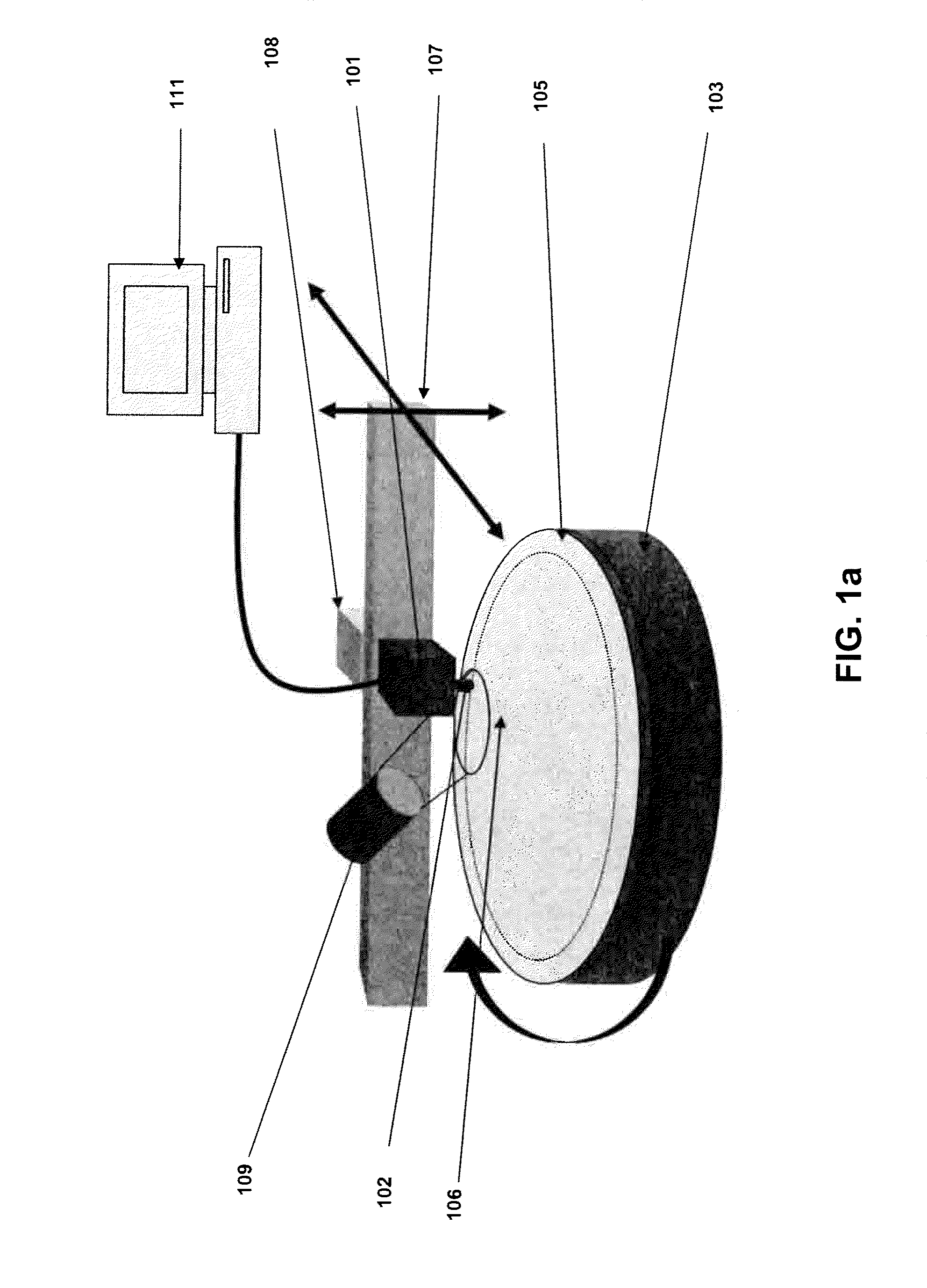
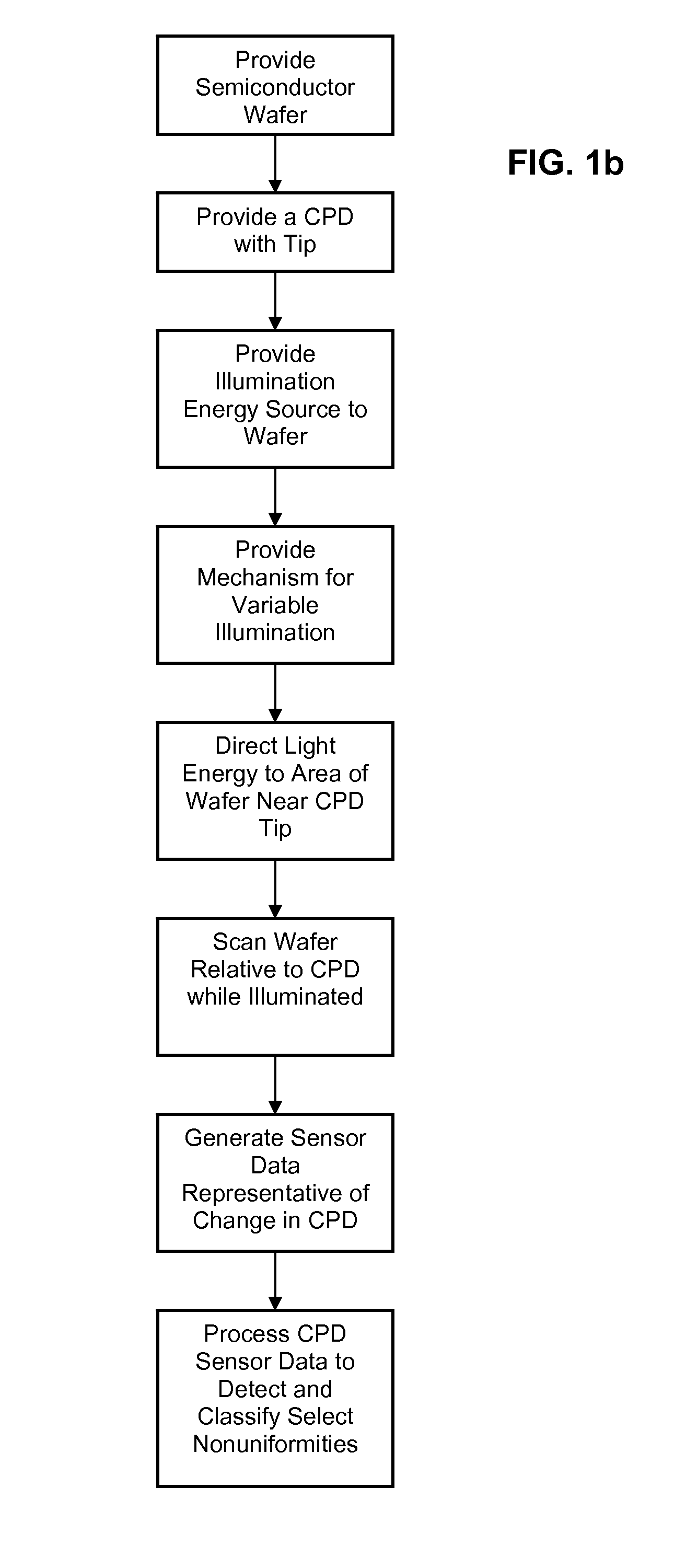
[0031]FIG. 3 illustrates non-vibrating contact potential difference images of a wafer 105. FIG. 3(a) is super-bandgap illumination, FIG. 3(b) is with no illumination and FIG. 3(c) is the difference between that shown in FIG. 3(a) and FIG. 3(b). The pattern in 3(c) is boron implanted into the wafer 105. The difference image shows a strong doping pattern and minimizes the signal from surface contaminants which are visible in (a) and (b).

[0032]FIG. 4 illustrates the non-vibrating contact potential difference images of the wafer 105 shown in FIGS. 3(a)-(c) with processing to identify regions of non-uniformity. The images have been processed by identifying regions of the image that fall above and below threshold values. Non-uniformity is clearly identified in FIG. 4(c), but is not distinguished from surface contamination in FIGS. 4(a) and 4(b).

[0033]There are many alternate mechanical configurations and scanning operations that would accomplish the same result as the embodiment described...


PUM


Abstract

A method and system for identifying a defect or contamination on the surface of a semiconductor or in a semiconductor. The method and system involves providing a semiconductor with a surface, such as a semiconductor wafer, providing a non-vibrating contact potential difference sensor, providing a source of illumination with controllable intensity or distribution of wavelengths, using the illumination source to provide controlled illumination of the surface of the wafer under or near the non-vibrating contact potential sensor probe tip, using the non-vibrating contact potential difference sensor to scan the wafer surface during controlled illumination, generating data representative of changes in contact potential difference across the wafer surface, and processing that data to identify a pattern characteristic of a defect or contamination.

Description

FIELD OF THE INVENTION[0001]The present invention is directed to methods and systems for the inspection of semiconductors and semiconductor surfaces. More particularly, the present invention is directed to a method and system for the characterization of non-uniformities through the use of a non-vibrating contact potential difference sensor in combination with a controllable illumination source to image and visualize the contact potential difference of the wafer surface.BACKGROUND OF THE INVENTION[0002]The function, reliability and performance of semiconductor devices depend on the use of semiconductor materials and surfaces which are clean and uniform. Billions of dollars and countless man-hours have been spent developing, characterizing, and optimizing systems and processes for fabricating and processing semiconductor materials. A primary goal of this activity has been the fabrication of materials and surfaces that are extremely clean and that have properties that are uniform, or v...

Claims


Application Information

Patent Timeline
Patent Type & Authority Patents(United States)
IPC IPC(8): G01R31/26
CPCG01N27/002G01R31/2656G01R31/2648H01L22/00
Inventor HAWTHORNE, JEFFREY ALANSTEELE, M. BRANDONYANG, YEYUANSCHULZE, MARK
Owner QCEPT INVESTMENTS LLC
Why Eureka
Try Eureka