
Semiconductor wafer boat for batch processing

a technology of semiconductors and wafers, applied in the direction of rigid containers, transportation and packaging, tray containers, etc., can solve the problems of high undesirable and costly, affecting the throughput in a commercial or production setting, excessively costly, etc., and achieve the effect of reducing the slippage effect of wafers and reducing friction

Inactive Publication Date: 2010-02-16
TOKYO ELECTRON LTD
View PDF43 Cites 18 Cited by
  • Summary
  • Abstract
  • Description
  • Claims
  • Application Information

AI Technical Summary

Benefits of technology

The present invention aims to prevent wafers from slipping and moving during a batch process in a wafer boat. This is achieved by recessing the surfaces of the wafer boat where the wafers rest, and creating a transition region around the wafers to prevent them from sliding outward. The slots in the boat are formed by notches in vertical support rods, with clearance for the wafers to be inserted. The wafers are then lowered onto the recessed areas of the supports, where they cannot slide off the boat. The invention ensures that wafers can only be removed from the boat if they are raised above the slots.

Problems solved by technology

This movement, or wafer slippage, mis-aligns the wafers 20 such that, when picked up by a transfer arm 27, a wafer 20 can strike one of the legs 12, which can cause the wafer to break or will allow the wafer to slide out of the boat before transfer, which is highly undesirable and costly.
This solution, while tolerable in a research or laboratory environment, impacts throughput in a commercial or production setting, which is excessively costly.

Method used


Image

  • Semiconductor wafer boat for batch processing
  • Semiconductor wafer boat for batch processing
  • Semiconductor wafer boat for batch processing

Examples


Embodiment Construction

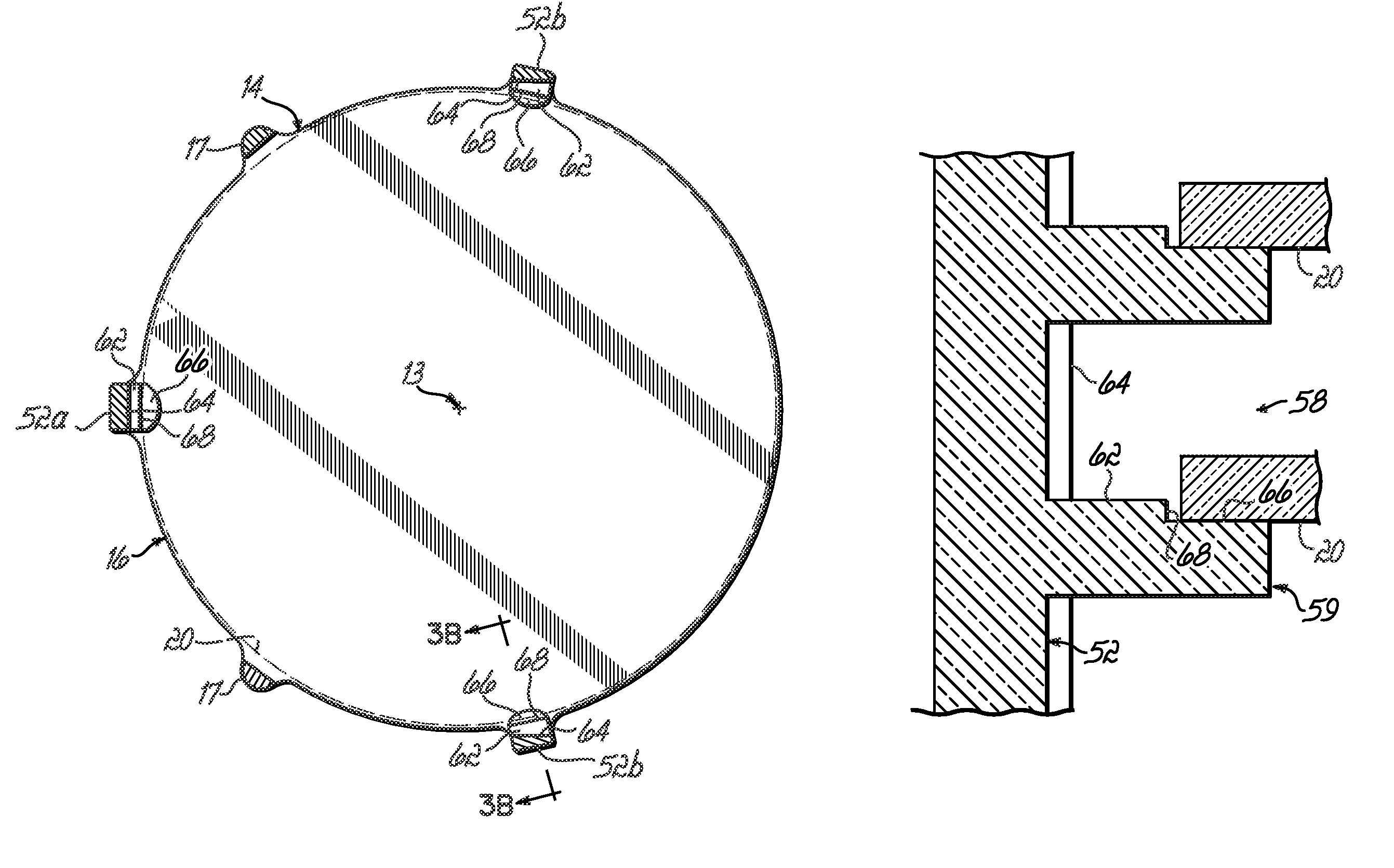
[0022]One embodiment of the present invention is illustrated in FIG. 3, which is representation of a boat 50 that has many details similar to that of boat 10 of FIG. 1. For example, the boat 50 includes a plurality of parallel vertical support members 52, which can be three or more in number, that are equally spaced from central vertical axis 13 and extend between base 14 and top plate 16. Further, a plurality of notches or slots 58 is provided in each of the vertical support members 52, mutually aligned with notches of the other members 52 and facing generally inwardly toward the central axis 13. Additional vertical structural members 17 without slots may also be provided to stiffen the boat 50.

[0023]As is shown in FIG. 3 and FIG. 3A, a plurality of wafers 20 are supported horizontally in the slots 58 of the members 52 with their centers aligned on the central axis 13. The members 52 include one or more rearward members 52a at the back of the boat, and two forward members 52b on th...


PUM


Abstract

A boat is provided for stacking semiconductor wafers vertically in processes in which low friction deposits may coat wafer supporting surfaces. In carbon processes, for example, low friction coatings can form that allow the wafers to slip sideways in the boat, leaving them sufficiently out of alignment to cause wafer breakage in handling. Typical boats for these processes having vertical legs, typically three or four in number, in which aligned notches support each of the wafers. The slots provide enough clearance around the edge of the wafer to facilitate loading and unloading of the wafers without wafer damage, as long as the wafers remain centered. For low friction process environments, each notch is provided with a shallow recess on which the edge of a wafer can rest. The recess adds a low step close to the wafer edge that resists horizontal sliding movement of the wafer. Wafers are loaded by inserting them into the boat in a plane spaced above the steps, then lowered onto the recesses.

Description

[0001]This invention relates to batch processing of semiconductor wafers and similar substrates, and more particularly to carbon deposition processing and other processes in which low friction materials deposit on surfaces within a wafer processing chamber.BACKGROUND OF THE INVENTION[0002]Semiconductor wafer processes commonly involve the exposure of surfaces of the wafers to processing gas in a processing chamber. Many of these processes treat the wafers in batch processes that simultaneously expose a plurality of wafers to the processing gas. In many typical batch treatment processes, the wafers are carried in boats that support the wafers in an array in which they are arranged in parallel rack-like structure. These boats include those in which horizontally oriented wafers are spaced in a vertical stack. A common boat may be formed of a set of parallel vertical rods having slots or notches evenly spaced along each of the rods. These notches are arranged in mutual alignment with th...

Claims


Application Information

Patent Timeline
Patent Type & Authority Patents(United States)
IPC IPC(8): A47G19/08
CPCH01L21/67309
Inventor HERZOG, FRANK
Owner TOKYO ELECTRON LTD
Learn More