Method and apparatus for measuring shape of heat treatment jig

a technology of heat treatment jig and measuring device, which is applied in the direction of mechanical measuring device, manufacturing tool, instruments, etc., can solve the problems of more damage or crystal defect, affecting measurement, and affecting the measurement, so as to reduce the damage or crystal defect of the wafer and the effect of easy and accurate measurement of the jig

Inactive Publication Date: 2010-02-23
AGC INC
View PDF10 Cites 0 Cited by
  • Summary
  • Abstract
  • Description
  • Claims
  • Application Information

AI Technical Summary

Benefits of technology

[0018]Considering the above circumstances, the present invention is made to solve the above problems, and it is an object of the present invention to provide in order to produce a heat treatment jig to be used for placing a wafer and to be used in a heat treatment apparatus in a semiconductor manufacturing process, a method and an apparatus for measuring the shape of the heat treatment jig, which can easily and accurately measure the jig to confirm the jig has a shape reducing damages or crystal defects of a wafer.
[0025]According to the invention of the first and fourth aspects, since the position of a supporting portion for a heat treatment jig is made to be the same as the position of a holding portion for the heat treatment jig in a vertical heat treatment apparatus at a time of shape measurement, deflection of the heat treatment jig by its own weight can be reproduced conveniently. Accordingly, at a time of producing a heat treatment jig to be used for placing a wafer and to be used in a vertical heat treatment apparatus in a semiconductor manufacturing process, it is easily and accurately measure the shape to confirm that the shape can reduce occurrence or damages or crystal defects in a wafer. Further, since the inclination and the parallelism with top surface of the heat treatment jig is determined not according to manufacturing accuracy of entire back surface but according to accuracy of portions in contact with the holding portion of the vertical heat treatment apparatus, it becomes possible to easily measure a manufacturing accuracy of a surface to be used for placing a wafer, in a state that the shape has little measurement error from the shape in actual use.

Problems solved by technology

There has been a problem that in a case where a wafer 3 is held by such a boat and subjected to a heat treatment, since the weight of the wafer 3 is supported at contact portions with the grooves 4 of the boat, when a heat is applied to the wafer 3, there occurs a positioning shift due to a thermal expansion difference between the materials of the wafer 3 and the boat or due to deflection of the wafer 3 by its own weight, or there forms a shearing stress of the wafer 3 by its own weight, and they cause damages or crystal defects (slip) in the wafer 3.
However, in a semiconductor manufacturing process, a treatment such as an anneal treatment in which the heat treatment temperature is at least 1,200° C., becomes widely used and defect-free requirement for wafers becomes more strict, and consequently, more damages or crystal defects are detected even with a heat treatment jig having a conventionally proposed shape.
This is because such conventionally proposed shapes of heat treatment jigs are ones considering only deformation of a wafer but not considering deformation of the heat treatment jig itself by its own weight, or deformation of the heat treatment jig in a higher temperature region.
Further, in a case of point-contact type profiler, the heat treatment jig is deformed by a contact pressure to prevent accurate measurement.
However, on a flat stage, manufacturing accuracy of the opposite surface of the jig, more specifically, parallelism, may affect the measurement, and accurate measurement becomes difficult.
However, such a adjustment requires excessive steps and significantly deteriorates productivity.

Method used


Image

  • Method and apparatus for measuring shape of heat treatment jig
  • Method and apparatus for measuring shape of heat treatment jig
  • Method and apparatus for measuring shape of heat treatment jig

Examples


example 1

[0048]As a comparison result of measurement of these two methods, the graph of FIG. 12 shows a measurement result of a heat treatment jig 5 by a conventional measurement method, and the graph of FIG. 13 shows a measurement result of the same heat treatment jig 5 by the method of the present invention. In FIGS. 12 and 13, a lateral axis represents an angle position in a circumferential direction of the heat treatment jig 5, and a vertical axis represents displacement amount (deflection amount) in relation to the angular position in the circumferential direction.

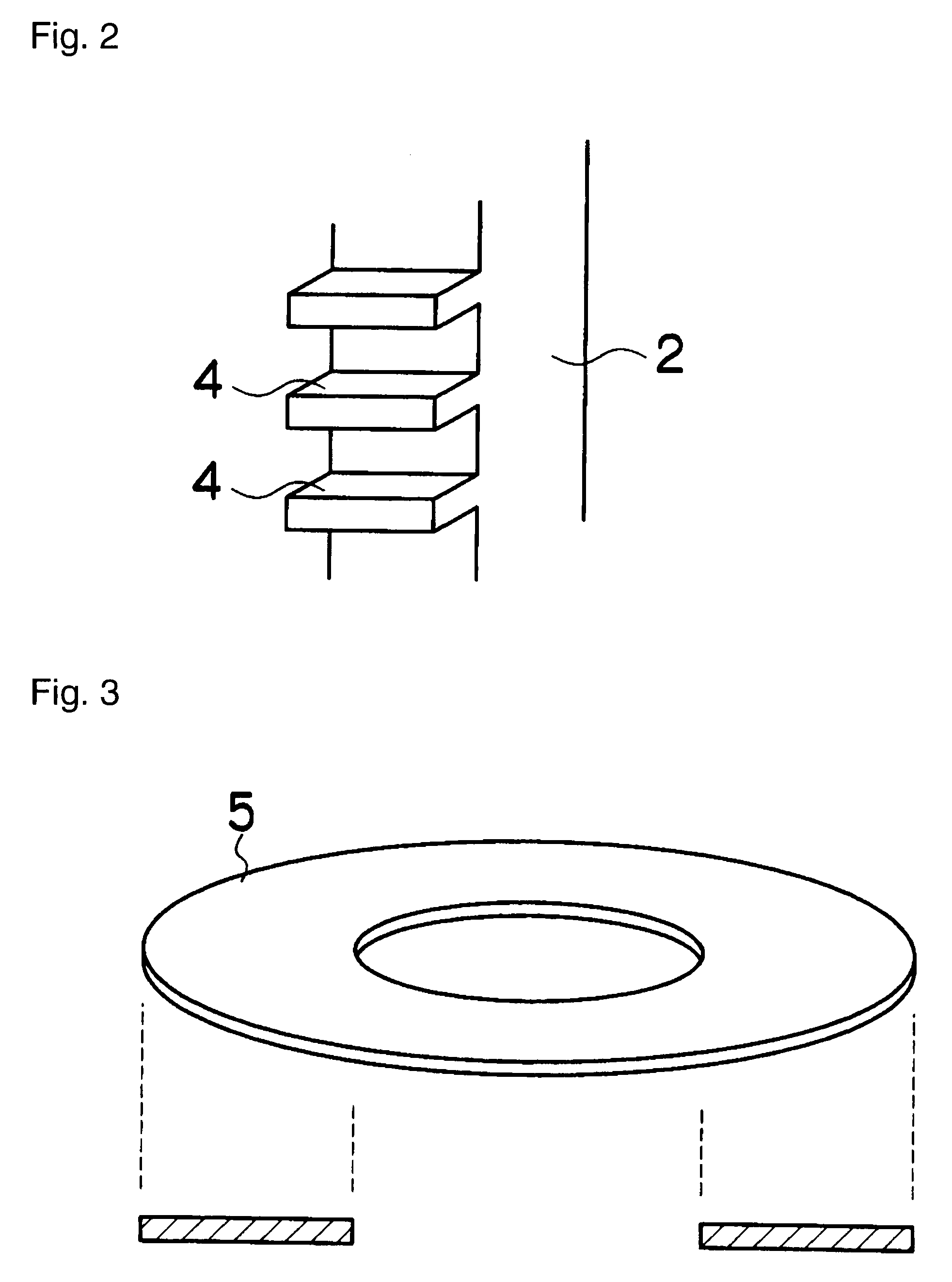
[0049]A heat treatment jig 5 used in these measurements has an outer diameter of 320 mm, an inner diameter of 200 mm and a thickness of 2.5 mm, its material is a sintered SiC coated with CVD-SiC of 50 μm thick. In the conventional measurement, a flatness tester (model: KS990X) manufactured by Anritsu Corporation is used as a measurement apparatus, and measurement of the heat treatment jig 5 is carried out as it was directly pl...

example 2

[0054]The graph shown in FIG. 14 and the graph shown in FIG. 15 show the above-mentioned measurement methods, wherein FIG. 14 shows a case of using a contact type dial gauge as means for detecting shape and accuracy and FIG. 15 shows a case of using a laser reflection type displacement as means for detecting shape and accuracy. In each of FIG. 14 and FIG. 15, the lateral axis represents an angular position in a circumferential direction of the heat treatment jig 5, and the vertical axis represents displacement amount (deflection amount) in relation to the angular position in the circumferential direction.

[0055]The heat treatment jig 5 used in this measurement has an outer diameter of 320 mm, an inner diameter of 200 mm and a thickness of 2.5 mm, and its material is a sintered SiC coated with CVD-SiC of 50 μm thick. As the measurement tool, a flatness tester (model: KS990X) manufactured by Anritsu Corporation was used, and SiC supporting portions 9, 18 and 27 (refer to FIG. 7) each f...


PUM

PropertyMeasurementUnit
temperatureaaaaaaaaaa
thicknessaaaaaaaaaa
thicknessaaaaaaaaaa

Abstract

A method for measuring the shape of a heating treatment jig to be held by a holding portion of a vertical heat treatment apparatus includes measuring the shape of the heat treatment jig in a state that the position of a supporting portion for supporting the heat treatment jig is set to be the same as the position of the holding portion for the heat treatment jig in the vertical heat treatment apparatus. The heat treatment jig can be used for placing a semiconductor wafer to be subjected to heat treatment.

Description

BACKGROUND OF THE INVENTION[0001]1. Field of the Invention[0002]The present invention relates to a heat treatment jig to be used for carrying out a heat treatment in a vertical heat treatment apparatus to be used in a semiconductor manufacturing process, and to a method and an apparatus for measuring the shape of such a heat treatment jig, to confirm that the jig has a shape reducing crystal defect or damage of a semiconductor wafer.[0003]2. Discussion of Background[0004]A process for treating a semiconductor wafer (hereinafter referred to as a “wafer”) in a semiconductor manufacturing process, includes a heat treatment process using high temperature such as an annealing treatment, an oxidation treatment or a diffusion treatment, and in such a heat treatment process, a vertical heat treatment apparatus is used according to upsizing of a wafer.[0005]In this type of vertical heat treatment apparatus, a holding jig named “boat” is used, which is constituted by a pair of end plates 1, 1...

Claims


Application Information

Patent Timeline
Patent Type & Authority Patents(United States)
IPC IPC(8): G01N3/00
CPCG01B21/20H01L21/67253H01L21/67303H01L21/67309
Inventor MISHIRO, HITOSHINAKAMURA, ATSUSHI
Owner AGC INC
Why Eureka
Try Eureka